Материал: DOC1228
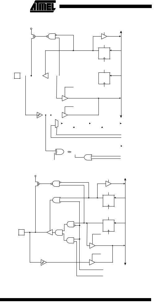
Port E Schematics |
Figure 72. Port E Schematic Diagram (Pin PE0) |
RD
MOS
PULL-
UP
RESET
R
Q D
DDE0
C
WD
RESET
R
PE0 
 Q D
Q D
PORTE0
C
RL
WP
RP
DATA BUS
WP: |
WRITE PORTE |
|
|
|
0 |
|
|
|
|
|
|
|
|
|
|
|
|
|
|
|
|
|
|
WD: |
WRITE DDRE |
1 |
|
|
|
|
NOISE CANCELER |
|
|
EDGE SELECT |
|
|
ICF1 |
||||||||||
RL: |
READ PORTE LATCH |
|
|
|
|
|
|
|
|
|
|
|
|
|
|
|
|
|
|||||
|
|
|
|
|
|
|
|
|
|
|
|
|
|
|
|||||||||
RP: |
READ PORTE PIN |
|
|
|
|
|
|
|
|
|
|
|
|
|
|
|
|
|
|
|
|
|
|
RD: |
READ DDRE |
|
|
|
|
|
|
|
|
|
|
|
|
|
|
|
|
|
|
|
|
|
|
|
|
|
|
|
|
|
|
|
|
ICNC1 |
|
|
|
|
ICES1 |
|
|
|
|||||
ACIC: COMPARATOR IC ENABLE |
|
|
|
|
|
|
|
|
|
|
|
|
|
|
|
|
ACIC |
||||||
ACO: COMPARATOR OUTPUT |
|
|
|
|
|
|
|
|
|
|
|
|
|
|
|
|
|
|
|
|
|||
|
|
|
|
|
|
|
|
|
|
|
|
|
|
|
|
|
|
|
|
|
|
|
ACO |
|
|
|
'1' |
|
|
|
|
|
|
|
|
|
|
|
INT2 |
||||||||
|
|
|
|
|
Q |
D |
|
|
|
|
|
|
|
||||||||||
|
|
|
|
|
|
|
|
|
|
|
|
|
PORTE0 |
|
|
|
|
|
|
|
|
||
|
|
|
|
|
|
|
|
|
|
|
|
|
C R |
|
|
|
|
|
|
|
|
|
|
|
|
|
|
|
|
|
|
|
|
|
|
|
|
|
|
|
|
|
|
|
|
||
|
|
|
|
|
|
|
|
|
|
|
|
|
|
|
|
|
|
|
|
|
|
||
HW CLEAR
SW CLEAR
ISC2
Figure 73. Port E Schematic Diagram (Pin PE1)
|
|
|
RD |
|
|
|
MOS |
|
|
|
|
|
PULL- |
|
|
|
|
|
UP |
|
|
|
|
|
|
|
RESET |
|
|
|
|
Q |
R |
D |
|
|
|
DDE1 |
|
||
|
|
|
|
|
|
|
|
|
C |
|
|
|
|
|
WD |
|
BUS |
|
|
|
RESET |
|
|
|
|
Q |
R |
D |
DATA |
|
|
PORTE1 |
|
||
|
|
|
C |
|
|
|
PE1 |
RL |
|
|
|
|
|
WP |
|
|
|
|
|
|
|
|
|
|
|
RP |
|
|
|
WP: |
WRITE PORTE |
SRE |
|
|
|
WD: |
WRITE DDRE |
|
|
|
|
RL: |
READ PORTE LATCH |
ALE |
|
|
|
RP: |
READ PORTE PIN |
|
|
||
RD: |
READ DDRE |
|
|
|
|
SRE: XRAM ENABLE |
|
|
|
|
|
ALE: ALE PULSE FROM XRAM |
|
|
|
|
|
106 ATmega161(L)
1228B–09/01
ATmega161(L)
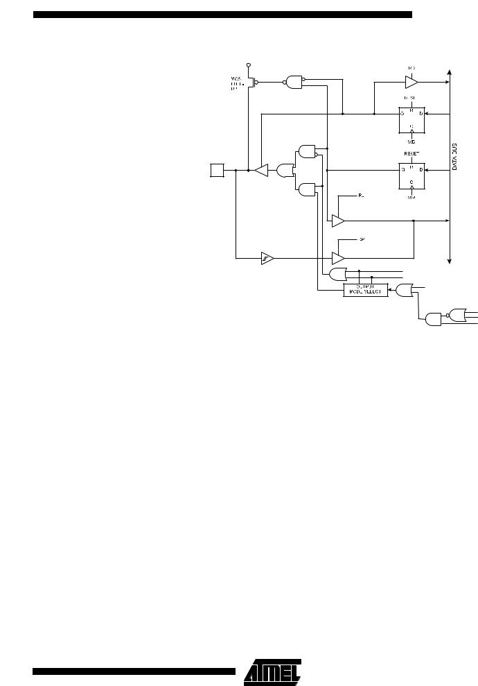
Figure 74. Port E Schematic Diagram (Pin PE2)
DDE2
PE2
PORTE2
WP: WRITE PORTE
WD: WRITE DDRE
RL: READ PORTE LATCH RP: READ PORTE PIN RD: READ DDRE
COM1B0
COM1B1
COMP. MATCH 1B
PWM10
PWM11
FOC1B
107
1228B–09/01
Memory
Programming
Boot Loader Support The ATmega161 provides a mechanism for downloading and uploading program code by the MCU itself. This feature allows flexible application software updates, controlled by the MCU using a Flash-resident Boot Loader program.
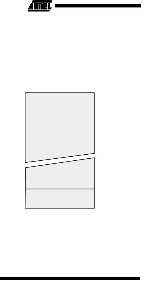
The ATmega161 Flash memory is organized in two main sections:
1.The Application Code section (address $0000 - $1DFF)
2.The Boot Loader section/Boot block (address $1E00 - $1FFF)
Figure 75. Memory Sections
Program Memory
$0000
Application Code section (7.5K x 16)
$1DFF
Boot Loader section $1E00 (512 x 16)
$1FFF
The Boot Loader program can use any available data interface and associated protocol, such as UART serial bus interface, to input or output program code and write (program) that code into the Flash memory or read the code from the program memory.
The program Flash memory is divided into pages that each contain 128 bytes. The Boot
Loader Flash section occupies eight pages from $1E00 to $1FFF by 16-bit words.
The Store Program Memory (SPM) instruction can access the entire Flash, but it can only be executed from the Boot Loader Flash section. If no Boot Loader capability is needed, the entire Flash is available for application code. The ATmega161 has two separate sets of Boot Lock bits that can be set independently. This gives the user a unique flexibility to select different levels of protection. The user can elect to:
108 ATmega161(L)
1228B–09/01

 ATmega161(L)
Entering the Boot Loader
Program
•Protect the entire Flash from a software update by the Boot Loader program
•Only protect the Boot Loader section from a software update by the Boot Loader program
•Only protect the Application Code section from a software update by the Boot Loader program
•Allow software update in the entire Flash
See Table 37 and Table 38 for further details. The Boot Lock bits can be set in software and in Serial or Parallel Programming mode, but they can only be cleared by a Chip Erase command.
Table 37. Boot Lock Bit0 Protection Modes (Application Code Section)(1)
BLB0 Mode |
BLB02 |
BLB01 |
Protection |
|
|
|
|
|
|
1 |
1 |
1 |
No restrictions for SPM, LPM accessing Application Code |
|
section |
||||
|
|
|
||
|
|
|
|
|
2 |
1 |
0 |
SPM is not allowed to write to the Application Code |
|
section. |
||||
|
|
|
||
|
|
|
|
|
|
|
|
SPM is not allowed to write to the Application Code |
|
3 |
0 |
0 |
section, and LPM executing from the Boot Loader section |
|
|
|
|
is not allowed to read from the Application Code section. |
|
|
|
|
|
|
4 |
0 |
1 |
LPM executing from the Boot Loader section is not |
|
allowed to read from the Application Code section. |
||||
|
|
|
||
|
|
|
|
|
Note: 1. “1” = unprogrammed, “0” = programmed |
||||
Table 38. Boot Lock Bit1 Protection Modes (Boot Loader Section)(1)
BLB1 Mode |
BLB12 |
BLB11 |
Protection |
|
|
|
|
|
|
1 |
1 |
1 |
No restrictions for SPM, LPM accessing Boot Loader |
|
section |
||||
|
|
|
||
|
|
|
|
|
2 |
1 |
0 |
SPM is not allowed to write to the Boot Loader section. |
|
|
|
|
|
|
|
|
|
SPM is not allowed to write to the Boot Loader section, |
|
3 |
0 |
0 |
and LPM executing from the Application Code section is |
|
|
|
|
not allowed to read from the Boot Loader section. |
|
|
|
|
|
|
4 |
0 |
1 |
LPM executing from the Application Code section is not |
|
allowed to read from the Boot Loader section. |
||||
|
|
|
||
|
|
|
|
|
Note: 1. “1” means unprogrammed, “0” means programmed |
||||
Entering the Boot Loader takes place by a jump or call from the application program. This may be initiated by some trigger such as a command received via UART or SPI interface. Alternatively, the Boot Reset Fuse (BOOTRST) can be programmed so that the reset vector is pointing to address $1E00 after a reset. In this case, the Boot Loader is started after the reset. After the application code is loaded, the program can start executing the application code. Note that the fuses cannot be changed by the MCU itself. This means that once the Boot Reset Fuse is programmed, the Reset Vector will always point to the Boot Loader Reset and the fuse can only be changed through the serial or parallel programming interface. The BOOTRST fuse can also be locked by programming LB1. When LB1 is programmed it is not possible to change the BOOTRST fuse unless a Chip Erase command is performed first.
109
1228B–09/01

Capabilities of the Boot
Loader
Table 39. Boot Reset Fuse, BOOTRST(1)
BOOTRST |
Reset Address |
|
|
1 |
Reset Vector = Application Reset (address $0000) |
|
|
0 |
Reset Vector = Boot Loader Reset (address $1E00) |
|
|
Note: 1. “1” means unprogrammed, “0” means programmed
The program code within the Boot Loader section has the ability to read from and write into the entire Flash, including the Boot Loader Memory. This allows the user to update both the Application code and the Boot Loader code that handles the software update. The Boot Loader can thus even modify itself, and it can also erase itself from the code if the feature is not needed anymore. Special care must be taken if the user allows the Boot Loader section to be updated by leaving Boot Lock bit11 unprogrammed. An accidental write to the Boot Loader itself can corrupt the entire Boot Loader, and further software updates might be impossible. If it is not needed to change the Boot Loader software itself, it is recommended that the Boot Lock bit 11 be programmed to protect the Boot Loader software from software changes.
Self-programming the
Flash
Setting the Boot Loader Lock Bits by SPM
Performing Page Erase by SPM
Programming of the Flash is executed one page at a time. The Flash page must be erased first for correct programming. The general Write Lock (Lock Bit 2) does not control the programming of the Flash memory by SPM instruction. Similarly, the Read/Write Lock (Lock Bit 1) does not control reading or writing by LPM/SPM, if it is attempted.
The program memory can only be updated page-by-page, not word by word. One page is 128 bytes (64 words). The program memory will be modified by first performing page erase, then by filling the temporary page buffer one word at a time using SPM, and then by executing page write. If only part of the page needs to be changed, the other parts must be stored (for example, in the temporary page buffer) before the erase, and then be rewritten. The temporary page buffer can be accessed in a random sequence. The CPU is halted both during page erase and during page write and the SPMEN bit in the SPMCR register will be auto-cleared. For future compatibility, however, it is recommended that the user software verify that the SPMEN bit is cleared before starting a new page erase, page write, or before writing the Lock Bits command (see code examples below). It is essential that the page address used in both the page erase and page write operation is addressing the same page.
To set the Boot Loader Lock bits, write the desired data to R0, write “1001” to SPMCR, and execute SPM within four clock cycles after writing SPMCR. The only accessible Lock bits are the Boot Lock bits that may prevent the Application Code and Boot Loader sections from any software update by the MCU. See Table 37 and Table 38 for how the different settings of the Boot Loader bits affect the Flash access.
Bit |
7 |
6 |
5 |
4 |
3 |
2 |
1 |
0 |
|
|
– |
– |
BLB12 |
BLB11 |
BLB02 |
BLB01 |
– |
– |
R0 |
|
|
|
|
|
|
|
|
|
|
If bit5 - bit2 in R0 is cleared (zero), the corresponding Boot Lock bit will be programmed if an SPM instruction is executed within four cycles after BLBSET and SPMEN are set in SPMCR.
To execute a page erase, set up the address in the Z-pointer, write “0011” to SPMCR, and execute SPM within four clock cycles after writing SPMCR. The data in R1 and R0 are ignored. The page address must be written to Z13:Z7. Other bits in the Z-pointer will be ignored during this operation.
110 ATmega161(L)
1228B–09/01