Материал: DOC1228

Port C |
|
|
|
|
|
|
|
|
|
|
|
|
|
|
|
|
|
|
|
|
|
|
|
Port C is an 8-bit bi-directional I/O port. |
|||||
|
Three I/O memory address locations are allocated for the Port C, one each for the Data |
||||
|
Register – PORTC, $15($35), Data Direction Register – DDRC, $14($34) and the Port C |
||||
|
Input Pins – PINC, $13($33). The Port C Input Pins address is read-only, while the Data |
||||
|
Register and the Data Direction Register are read/write. |
||||
|
All port pins have individually selectable pull-up resistors. The Port C output buffers can |
||||
|
sink 20 mA and thus drive LED displays directly. When pins PC0 to PC7 are used as |
||||
|
inputs and are externally pulled low, they will source current if the internal pull-up resis- |
||||
|
tors are activated. |
||||
|
The Port C pins have alternate functions related to the optional external memory inter- |
||||
|
face. Port C can be configured to be the high-order address byte during accesses to |
||||
|
external data memory. |
||||
|
When Port C is set to the alternate function by the SRE (External SRAM Enable) bit in |
||||
|
the MCUCR (MCU Control Register), the alternate settings override the Data Direction |
||||
|
Register. |
||||
Port C Data Register – PORTC
Port C Data Direction Register
– DDRC
Port C Input Pins Address –
PINC
Bit |
7 |
6 |
5 |
4 |
3 |
2 |
1 |
0 |
|
|
||||
$15 ($35) |
PORTC7 |
PORTC6 |
PORTC5 |
|
PORTC4 |
PORTC3 |
|
PORTC2 |
|
PORTC1 |
|
PORTC0 |
|
PORTC |
|
|
|
|
|
|
|
|
|
|
|
|
|
|
|
Read/Write |
R/W |
R/W |
R/W |
|
R/W |
R/W |
|
R/W |
|
R/W |
|
R/W |
|
|
Initial Value |
0 |
0 |
0 |
0 |
0 |
0 |
0 |
0 |
|
|
||||
Bit |
7 |
6 |
5 |
4 |
3 |
2 |
1 |
0 |
|
|
||||
|
|
|
|
|
|
|
|
|
|
|
|
|
|
|
$14 ($34) |
DDC7 |
DDC6 |
DDC5 |
|
DDC4 |
DDC3 |
|
DDC2 |
|
DDC1 |
|
DDC0 |
|
DDRC |
|
|
|
|
|
|
|
|
|
|
|
|
|
|
|
Read/Write |
R/W |
R/W |
R/W |
|
R/W |
R/W |
|
R/W |
|
R/W |
|
R/W |
|
|
Initial Value |
0 |
0 |
0 |
0 |
0 |
0 |
0 |
0 |
|
|
||||
Bit |
7 |
6 |
5 |
4 |
3 |
2 |
1 |
0 |
|
|
||||
|
|
|
|
|
|
|
|
|
|
|
|
|
|
|
$13 ($33) |
PINC7 |
PINC6 |
PINC5 |
|
PINC4 |
PINC3 |
|
PINC2 |
|
PINC1 |
|
PINC0 |
|
PINC |
|
|
|
|
|
|
|
|
|
|
|
|
|
|
|
Read/Write |
R |
R |
R |
|
R |
R |
|
R |
|
R |
|
R |
|
|
Initial Value |
N/A |
N/A |
N/A |
|
N/A |
N/A |
|
N/A |
|
N/A |
|
N/A |
|
|
The Port C Input Pins address (PINC) is not a register; this address enables access to the physical value on each Port C pin. When reading PORTC, the Port C Data Latch is read and when reading PINC, the logical values present on the pins are read.
Port C as General Digital I/O All eight pins in Port C have equal functionality when used as digital I/O pins.
PCn, general I/O pin: The DDCn bit in the DDRC register selects the direction of this pin. If DDCn is set (one), PCn is configured as an output pin. If DDCn is cleared (zero), PCn is configured as an input pin. If PORTCn is set (one) when the pin is configured as an input pin, the MOS pull-up resistor is activated. To switch the pull-up resistor off, PORTCn has to be cleared (zero) or the pin has to be configured as an output pin. The Port C pins are tri-stated when a reset condition becomes active, even if the clock is not running.
96 ATmega161(L)
1228B–09/01
ATmega161(L)
Table 32. DDCn Effects on Port C Pins(1)
DDCn |
PORTCn |
I/O |
Pull-up |
Comment |
|
|
|
|
|
0 |
0 |
Input |
No |
Tri-state (high-Z) |
|
|
|
|
|
0 |
1 |
Input |
Yes |
PCn will source current if ext. pulled low |
|
|
|
|
|
1 |
0 |
Output |
No |
Push-pull Zero Output |
|
|
|
|
|
1 |
1 |
Output |
No |
Push-pull One Output |
|
|
|
|
|
|
Note: 1. n: 7, 6,…0, pin number |
|||||||||||||||||||||||||
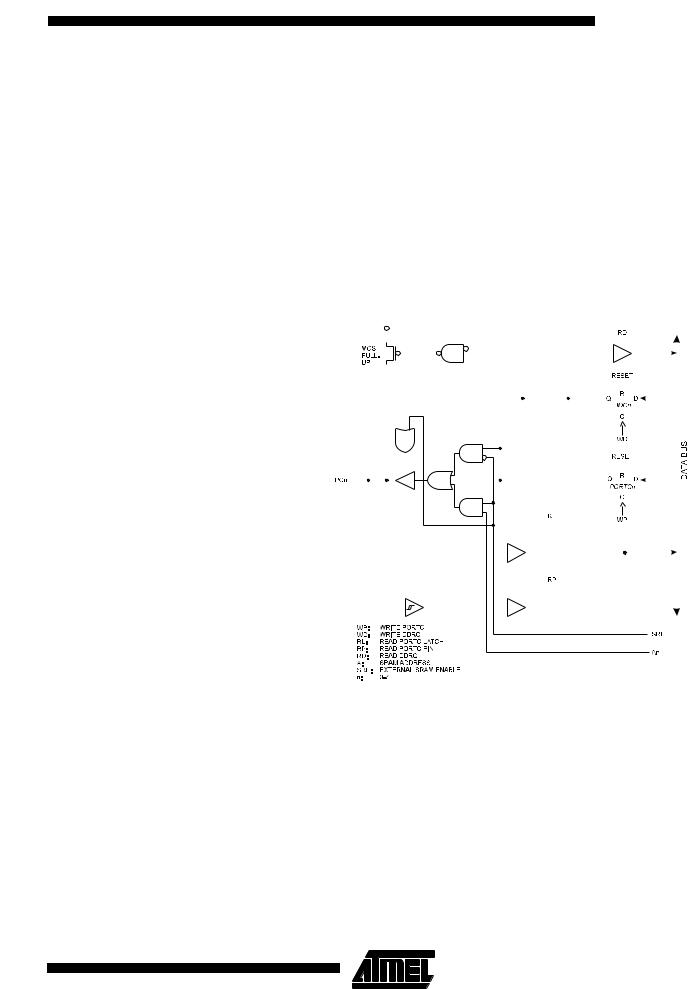
Port C Schematics |
Note that all port pins are synchronized. The synchronization latch is, however, not |
|||||||||||||||||||||||||
|
shown in the figure. |
|||||||||||||||||||||||||
|
Figure 64. Port C Schematic Diagram (Pins PC0 - PC7) |
|||||||||||||||||||||||||
|
|
|
|
|
|
|
|
|
|
|
|
|
|
|
|
|
|
|
|
|
|
|
|
|
|
|
|
|
|
|
|
|
|
|
|
|
|
|
|
|
|
|
|
|
|
|
|
|
|
|
|
|
|
|
|
|
|
|
|
|
|
|
|
|
|
|
|
|
|
|
|
|
|
|
|
|
|
|
|
|
|
|
|
|
|
|
|
|
|
|
|
|
|
|
|
|
|
|
|
|
|
|
|
|
|
|
|
|
|
|
|
|
|
|
|
|
|
|
|
|
|
|
|
|
|
|
|
|
|
|
|
|
|
|
|
|
|
|
|
|
|
|
|
|
|
|
|
|
|
|
|
|
|
|
|
|
|
|
|
|
|
|
|
|
|
|
|
|
|
|
|
|
|
|
|
|
|
|
|
|
|
|
|
|
|
|
|
|
|
|
|
|
|
|
|
|
|
|
|
|
|
|
|
|
|
|
|
|
|
|
|
|
|
|
|
|
|
|
|
|
|
|
|
|
|
|
|
|
|
|
|
|
|
|
|
|
|
|
|
|
|
|
|
|
|
|
|
|
|
|
|
|
|
|
|
|
|
|
|
|
|
|
|
|
|
|
|
|
|
|
|
|
|
|
|
|
|
|
|
|
|
|
|
|
|
|
|
|
|
|
|
|
|
|
|
|
|
|
|
|
|
|
|
|
|
|
|
|
|
|
|
|
|
|
|
|
|
|
|
|
|
|
|
|
|
|
|
|
|
|
|
|
|
|
|
|
|
|
|
|
|
|
|
|
|
|
|
|
|
|
|
|
|
|
|
|
|
|
|
|
|
|
|
|
|
|
|
|
|
|
|
|
|
|
|
|
|
|
|
|
|
|
|
|
|
|
|
|
|
|
|
|
|
|
|
|
|
|
|
|
|
|
|
|
|
|
|
|
|
|
|
|
|
|
|
|
|
|
|
|
|
|
|
|
|
|
|
|
|
|
|
|
|
|
|
|
|
|
|
|
|
|
|
|
|
|
|
|
|
|
|
|
|
|
|
|
|
|
|
|
|
|
|
|
|
|
|
|
|
|
|
|
|
|
|
|
|
|
|
|
|
|
|
|
|
|
|
|
|
|
|
|
|
|
|
|
|
|
|
|
|
|
|
|
|
|
|
|
|
|
|
|
|
|
|
|
|
|
|
|
|
|
|
|
|
|
|
|
|
|
|
|
|
|
|
|
|
|
|
|
|
|
|
|
|
|
|
|
|
|
|
|
|
|
|
|
|
|
|
|
|
|
|
|
|
|
|
|
|
|
|
|
|
|
|
|
|
|
|
|
|
|
|
|
|
|
|
|
|
|
|
|
|
|
|
|
|
|
|
|
|
|
|
|
|
|
|
|
|
|
|
|
|
|
|
|
|
|
|
|
97
1228B–09/01

Port D |
|
|
|
|
|
|
|
|
|
|
|
|
|
|
|
|
|
|
|
|
|
|
|
|
|
|
|
|
|
|
|
|
|
|
|
|
|
|
|
Port D is an 8-bit bi-directional I/O port with internal pull-up resistors. |
|||||||||
|
Three I/O address locations are allocated for the Port D, one each for the Data Register |
||||||||
|
– PORTD, $12($32), Data Direction Register – DDRD, $11($31) and the Port D Input |
||||||||
|
Pins – PIND, $10($30). The Port D Input Pins address is read-only, while the Data Reg- |
||||||||
|
ister and the Data Direction Register are read/write. |
||||||||
|
The Port D output buffers can sink 20 mA. As inputs, Port D pins that are externally |
||||||||
|
pulled low will source current if the pull-up resistors are activated. |
||||||||
|
Some Port D pins have alternate functions as shown in Table 33. |
||||||||
|
Table 33. Port D Pin Alternate Functions |
||||||||
|
|
|
|
||||||
|
Port Pin |
|
Alternate Function |
||||||
|
|
|
|
||||||
|
PD0 |
|
RXD0 (UART0 Input Line) |
||||||
|
|
|
|
||||||
|
PD1 |
|
TXD0 (UART0 Output Line) |
||||||
|
|
|
|
||||||
|
PD2 |
|
INT0 (External Interrupt0 Input) |
||||||
|
|
|
|
||||||
|
PD3 |
|
INT1 (External Interrupt1 Input) |
||||||
|
|
|
|
||||||
|
PD3 |
|
TOSC1 (RTC Oscillator Timer/Counter2) |
||||||
|
|
|
|
||||||
|
PD5 |
|
TOSC2 (RTC Oscillator Timer/Counter2)/OC1A (Timer/Counter1 Output |
||||||
|
|
CompareA Match Output) |
|||||||
|
|
|
|||||||
|
|
|
|
|
|
||||
|
PD6 |
|
|
|
(Write Strobe to External Memory) |
||||
|
WR |
||||||||
|
|
|
|
|
|||||
|
PD7 |
|
|
(Read Strobe to External Memory) |
|||||
|
RD |
||||||||
|
|
|
|
|
|
|
|
|
|
When the PD5 pin is used for the alternate function (OC1A), the DDRD and PORTD registers have to be set according to the alternate function description.
Port D Data Register – PORTD
Port D Data Direction Register
– DDRD
Port D Input Pins Address –
PIND
Bit |
7 |
6 |
5 |
4 |
3 |
|
2 |
|
1 |
0 |
|
$12 ($32) |
PORTD7 |
PORTD6 |
PORTD5 |
PORTD4 |
PORTD3 |
PORTD2 |
PORTD1 |
PORTD0 |
PORTD |
||
|
|
|
|
|
|
|
|
|
|
|
|
Read/Write |
R/W |
R/W |
R/W |
R/W |
R/W |
R/W |
R/W |
R/W |
|
||
Initial Value |
0 |
0 |
0 |
0 |
0 |
|
0 |
|
0 |
0 |
|
Bit |
7 |
6 |
5 |
4 |
3 |
|
2 |
|
1 |
0 |
|
|
|
|
|
|
|
|
|
|
|
|
|
$11 ($31) |
DDD7 |
DDD6 |
DDD5 |
DDD4 |
DDD3 |
DDD2 |
DDD1 |
DDD0 |
DDRD |
||
|
|
|
|
|
|
|
|
|
|
|
|
Read/Write |
R/W |
R/W |
R/W |
R/W |
R/W |
R/W |
R/W |
R/W |
|
||
Initial Value |
0 |
0 |
0 |
0 |
0 |
|
0 |
|
0 |
0 |
|
Bit |
7 |
6 |
5 |
4 |
3 |
|
2 |
|
1 |
0 |
|
|
|
|
|
|
|
|
|
|
|
|
|
$10 ($30) |
PIND7 |
PIND6 |
PIND5 |
PIND4 |
PIND3 |
|
PIND2 |
|
PIND1 |
PIND0 |
PIND |
|
|
|
|
|
|
|
|
|
|
|
|
Read/Write |
R |
R |
R |
R |
R |
R |
R |
R |
|
||
Initial Value |
N/A |
N/A |
N/A |
N/A |
N/A |
N/A |
N/A |
N/A |
|
||
The Port D Input Pins address (PIND) is not a register; this address enables access to the physical value on each Port D pin. When reading PORTD, the Port D Data Latch is read and when reading PIND, the logical values present on the pins are read.
Port D as General Digital I/O PDn, general I/O pin: The DDDn bit in the DDRD register selects the direction of this pin. If DDDn is set (one), PDn is configured as an output pin. If DDDn is cleared (zero), PDn is configured as an input pin. If PORTDn is set (one) when configured as an input pin, the MOS pull-up resistor is activated. To switch the pull-up resistor off, the PORTDn has
98 ATmega161(L)
1228B–09/01

 ATmega161(L)
to be cleared (zero) or the pin has to be configured as an output pin. The Port D pins are tri-stated when a reset condition becomes active, even if the clock is not running.
Table 34. DDDn Bits on Port D Pins(1)
DDDn |
|
PORTDn |
I/O |
Pull-up |
Comment |
|
|
|
|
|
|
0 |
|
0 |
Input |
No |
Tri-state (high-Z) |
|
|
|
|
|
|
0 |
|
1 |
Input |
Yes |
PDn will source current if ext. pulled low. |
|
|
|
|
|
|
1 |
|
0 |
Output |
No |
Push-pull Zero Output |
|
|
|
|
|
|
1 |
|
1 |
Output |
No |
Push-pull One Output |
|
|
|
|
|
|
Notes: |
1. n: 7,6…0, pin number |
|
|
||
Alternate Functions of Port D The alternate pin configuration is as follows:
• RD – Port D, Bit 7
RD is the external data memory read control strobe.
• WR – Port D, Bit 6
WR is the external data memory write control strobe.
• OC1 – Port D, Bit 5
OC1, Output compare match output: The PD5 pin can serve as an external output when the Timer/Counter1 compare matches. The PD5 pin has to be configured as an output (DDD5 set [one]) to serve this function. See “Timer/Counter1” on page 49 for further details and how to enable the output. The OC1 pin is also the output pin for the PWM mode timer function.
• TOSC1/TOSC2 – Port D, Bits 5 and 4
When the AS2 bit in ASSR is set (one) to enable asynchronous clocking of Timer/Counter2, pins PD5 and PD4 are disconnected from the port. In this mode, a crystal oscillator is connected to the pins and the pins cannot be used as I/O pins.
• INT1 – Port D, Bit 3
INT1, External Interrupt source 1: The PD3 pin can serve as an external interrupt source to the MCU. See “MCU Control Register – MCUCR” on page 34 for further details.
• INT0 – Port D, Bit 2
INT0, External Interrupt source 0: The PD2 pin can serve as an external interrupt source to the MCU. See “MCU Control Register – MCUCR” on page 34 for further details.
• TXD0 – Port D, Bit 1
Transmit Data (Data output pin for the UART0). When the UART0 transmitter is enabled, this pin is configured as an output regardless of the value of DDRD1.
• RXD0 – Port D, Bit 0
Receive Data (Data input pin for the UART0). When the UART receiver is enabled, this pin is configured as an input regardless of the value of DDRD0. When the UART0 forces this pin to be an input, a logical “1” in PORTD0 will turn on the internal pull-up.
99
1228B–09/01
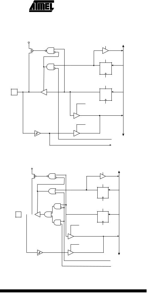
Port D Schematics |
|
|
|
|
|
|
|
|
|
|
|
|
|
|
|
|
|
|
|
|
|
|
|
Note that all port pins are synchronized. The synchronization latches are, however, not |
|||||
|
shown in the figures. |
||||
|
Figure 65. Port D Schematic Diagram (Pin PD0) |
||||
|
|
RD |
|
MOS |
|
|
PULL- |
|
|
UP |
|
|
|
RESET |
|
Q |
D |
|
|
DDD0 |
|
|
C |
|
|
WD |
|
|
RESET |
PD0 |
Q |
D |
|
PORTD0 |
|
|
|
C |
|
RL |
WP |
|
|
|
|
|
RP |
WP: |
WRITE PORTD |
RXEN0 |
|
||
WD: |
WRITE DDRD |
|
RL: |
READ PORTD LATCH |
RXD0 |
RP: |
READ PORTD PIN |
|
RD: |
READ DDRD |
|
RXD0: |
UART0 RECEIVE DATA |
|
RXEN0: |
UART0 RECEIVE ENABLE |
|
DATA BUS
Figure 66. Port D Schematic Diagram (Pin PD1)
RD
MOS
PULL-
UP
RESET
R
Q D
DDD1
C
WD
RESET
R PD1 
 Q D
Q D
PORTD1
C
RL
WP
DATA BUS
RP
WP: |
WRITE PORTD |
WD: |
WRITE DDRD |
RL: |
READ PORTD LATCH |
RP: |
READ PORTD PIN |
RD: |
READ DDRD |
TXD0: |
UART0 TRANSMIT DATA |
TXEN0: |
UART0 TRANSMIT ENABLE |
TXEN0
TXD0
100 ATmega161(L)
1228B–09/01