Материал: DOC1228
ATmega161(L)
• RXD1/AIN0 – Port B, Bit 2
AIN0, Analog Comparator Positive Input. This pin also serves as the positive input of the on-chip Analog Comparator.
RXD1, Receive Data (Data input pin for the UART1). When the UART1 receiver is enabled, this pin is configured as an input regardless of the value of DDRB2. When the UART1 forces this pin to be an input, a logical “1” in PORTB2 will turn on the internal pull-up.
• OC2/T1 – Port B, Bit 1
T1: Timer/Counter1 counter source. See “Timer/Counter1” on page 49 for further details.
OC2, Output compare match output: The PB1 pin can serve as an external output when the Timer/Counter2 compare matches. The PB1 pin has to be configured as an output (DDB1 set [one]) to serve this function. See “8-bit Timer/Counters T/C0 and T/C2” on page 40 for further details. The OC2 pin is also the output pin for the PWM mode timer function.
• OC0/T0 – Port B, Bit 0
T0: Timer/Counter0 counter source. See “8-bit Timer/Counters T/C0 and T/C2” on page 40 further details.
OC0, Output compare match output: The PB0 pin can serve as an external output when the Timer/Counter0 compare matches. The PB0 pin has to be configured as an output (DDB0 set [one]) to serve this function. See “8-bit Timer/Counters T/C0 and T/C2” on page 40 for further details and how to enable the output. The OC0 pin is also the output pin for the PWM mode timer function.
91
1228B–09/01
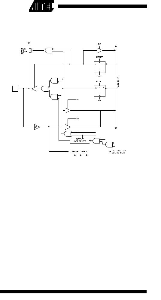
Port B Schematics
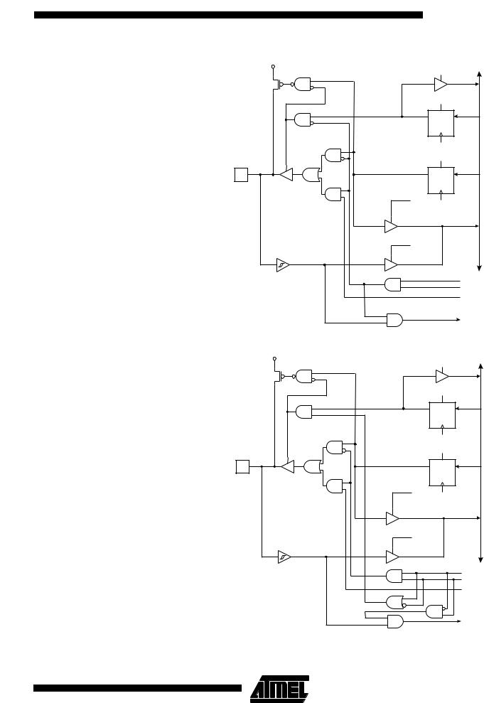
Note that all port pins are synchronized. The synchronization latches are, however, not shown in the figures.
Figure 57. Port B Schematic Diagram (Pins PB0 and PB1)
DDBn
PBn
PORTBn
WP: |
WRITE PORTB |
COMx0 |
|
COMx1 |
|||
WD: |
WRITE DDRB |
||
|
|||
RL: |
READ PORTB LATCH |
COMP. MATCH x |
|
RP: |
READ PORTB PIN |
||
|
|||
RD: |
READ DDRB |
PWMx |
n:0,1
x: 0,2 |
|
|
|
|
|
|
FOCx |
|
|
|
|
|
|
|
|
|
|
|
|
|
|
|
|
|
|
|
|
|
|
|
|
|
|
|
|
|
|
|
|
CSn2 CSn1 CSn0
92 ATmega161(L)
1228B–09/01
ATmega161(L)
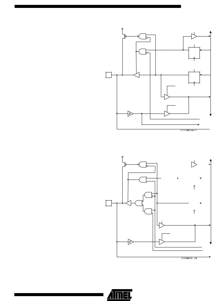
Figure 58. Port B Schematic Diagram (Pin PB2)
|
|
RD |
|
MOS |
|
|
PULL- |
|
|
UP |
|
|
|
RESET |
|
Q |
D |
|
|
DDB2 |
|
|
C |
|
|
WD |
|
|
RESET |
PB2 |
Q |
D |
|
PORTB2 |
|
|
|
C |
|
RL |
WP |
|
|
|
RP
RXEN1 |
RXD1 |
WP: |
WRITE PORTB |
WD: |
WRITE DDRB |
RL: |
READ PORTB LATCH |
RP: |
READ PORTB PIN |
RD: |
READ DDRB |
RXD1: |
UART1 RECEIVE DATA |
RXEN1: |
UART1 RECEIVE ENABLE |
AIN0: |
ANALOG COMPARATOR POSITIVE INPUT |
DATA BUS
 AIN0
AIN0
Figure 59. Port B Schematic Diagram (Pin PB3)
MOS
PULL-
UP
PB3
|
|
|
|
|
RD |
|
|
|
|
|
||
|
|
|
|
|
|
|
|
|
|
|
|
|
|
|
|
|
RESET |
|
|
|
|
|
|||
|
|
|
|
|
|
|
|
|
|
|
|
|
|
|
|
|
Q |
R |
D |
|
|
|
|
||
|
|
|
|
DDB3 |
|
|
|
|
||||
|
|
|
|
|
|
|
|
|
|
|||
|
|
|
|
|
C |
|
|
|
|
|
||
|
|
|
|
|
|
|
|
|
|
|
|
|
|
|
|
|
|
WD |
|
|
|
|
BUS |
||
|
|
|
|
RESET |
|
|
|
|
||||
|
|
|
|
|
|
|
|
DATA |
||||
|
|
|
|
|
|
|
|
|
|
|
|
|
|
|
|
|
Q |
R |
D |
||||||
|
|
|
|
PORTB3 |
|
|
|
|
||||
|
|
|
|
|
C |
|
|
|
|
|
||
|
|
RL |
|
|
|
|
|
|
|
|
|
|
|
|
|
WP |
|
|
|
|
|
||||
|
|
|
|
|
|
|
|
|
|
|
|
|
RP
TXEN1
TXD1
WP: |
WRITE PORTB |
|
WD: |
WRITE DDRB |
AIN1 |
RL: |
READ PORTB LATCH |
|
RP: |
READ PORTB PIN |
|
RD: |
READ DDRB |
|
TXD1: |
UART1 TRANSMIT DATA |
|
TXEN1: |
UART1 TRANSMIT ENABLE |
|
AIN1: |
ANALOG COMPARATOR NEGATIVE INPUT |
|
93
1228B–09/01
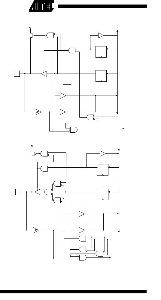
Figure 60. Port B Schematic Diagram (Pin PB4)
|
|
RD |
|
MOS |
|
|
PULL- |
|
|
UP |
|
|
|
RESET |
|
Q |
D |
|
|
DDB4 |
|
|
C |
|
|
WD |
|
|
RESET |
PB4 |
Q |
D |
|
PORTB4 |
|
|
|
C |
|
RL |
WP |
|
|
|
RP
DATA BUS
WP: |
WRITE PORTB |
WD: |
WRITE DDRB |
RL: |
READ PORTB LATCH |
RP: |
READ PORTB PIN |
RD: |
READ DDRB |
MSTR: |
SPI MASTER ENABLE |
SPE: |
SPI ENABLE |
MSTR
SPE
 SPI SS
Figure 61. Port B Schematic Diagram (Pin PB5)
|
|
|
RD |
|
|
|
MOS |
|
|
|
|
|
PULL- |
|
|
|
|
|
UP |
|
|
|
|
|
|
RESET |
|
|
|
|
|
Q |
R |
D |
|
|
|
DDB5 |
|
||
|
|
|
|
|
|
|
|
|
C |
|
|
|
|
|
WD |
|
BUS |
|
|
RESET |
|
||
PB5 |
|
Q |
R |
D |
DATA |
|
|
PORTB5 |
|
||
|
|
|
C |
|
|
|
RL |
|
WP |
|
|
|
|
|
|
|
|
|
RP |
|
|
|
|
WP: |
WRITE PORTB |
|
|
|
MSTR |
WD: |
WRITE DDRB |
|
|
|
|
|
|
|
SPE |
||
RL: |
READ PORTB LATCH |
|
|
|
|
|
|
|
SPI MASTER |
||
RP: |
READ PORTB PIN |
|
|
|
|
RD: |
READ DDRB |
|
|
|
OUT |
SPE: |
SPI ENABLE |
|
|
|
|
MSTR MASTER SELECT |
|
|
|
|
|
|
|
|
|
|
SPI SLAVE |
|
|
|
|
|
IN |
94 ATmega161(L)
1228B–09/01
ATmega161(L)
Figure 62. Port B Schematic Diagram (Pin PB6)
|
|
|
RD |
|
|
|
MOS |
|
|
|
|
|
PULL- |
|
|
|
|
|
UP |
|
|
|
|
|
|
RESET |
|
|
|
|
|
Q |
R |
D |
|
|
|
DDB6 |
|
||
|
|
|
|
|
|
|
|
|
C |
|
|
|
|
|
WD |
|
BUS |
|
|
RESET |
|
||
PB6 |
|
Q |
R |
D |
DATA |
|
|
PORTB6 |
|
||
|
|
|
C |
|
|
|
RL |
|
WP |
|
|
|
|
|
|
|
|
|
RP |
|
|
|
|
WP: WRITE PORTB
WD: WRITE DDRB
RL: READ PORTB LATCH RP: READ PORTB PIN RD: READ DDRB
SPE: SPI ENABLE MSTR MASTER SELECT
MSTR
SPE
SPI SLAVE OUT
SPI MASTER IN
Figure 63. Port B Schematic Diagram (Pin PB7)
|
|
|
RD |
|
|
|
MOS |
|
|
|
|
|
PULL- |
|
|
|
|
|
UP |
|
|
|
|
|
|
RESET |
|
|
|
|
|
Q |
R |
D |
|
|
|
DDB7 |
|
||
|
|
|
|
|
|
|
|
|
C |
|
|
|
|
|
WD |
|
BUS |
|
|
RESET |
|
||
|
|
|
DATA |
||
PB7 |
|
Q |
R |
D |
|
|
|
PORTB7 |
|
||
|
|
|
C |
|
|
|
RL |
|
WP |
|
|
|
|
|
|
|
|
|
RP |
|
|
|
|
WP: |
WRITE PORTB |
|
|
|
MSTR |
WD: |
WRITE DDRB |
|
|
|
|
|
|
|
SPE |
||
RL: |
READ PORTB LATCH |
|
|
|
|
|
|
|
SPI ClLOCK |
||
RP: |
READ PORTB PIN |
|
|
|
|
RD: |
READ DDRB |
|
|
|
OUT |
SPE: |
SPI ENABLE |
|
|
|
|
MSTR MASTER SELECT |
|
|
|
|
|
|
|
|
|
|
SPI CLOCK |
|
|
|
|
|
IN |
95
1228B–09/01