Материал: DOC1228

 ATmega161(L)
Internal Voltage
Reference
Voltage Reference Enable Signals and Startup Time
1228B–09/01
ATmega161 features an internal voltage reference with a nominal voltage of 1.22V. This reference is used for Brown-out Detection and it can be used as an input to the Analog Comparator.
The voltage reference has a start-up time that may have an influence on the way it should be used. The maximum start-up time is TBD. To save power, the reference is on during the following situations only:
1.When BOD is enabled (by programming the BODEN fuse)
2.When the bandgap reference is connected to the Analog Comparator (by setting the AINBG bit in ACSR)
Thus, when BOD is not enabled, after setting the AINBG bit, the user must always allow the reference to start up before the output from the Analog Comparator is used. The bandgap reference uses approximately 10 µA, and to reduce the power consumption in Power-down mode, the user can turn off the reference when entering this mode.
81
Interface to External Memory
MCU Control Register –
MCUCR
Extended MCU Control
Register – EMCUCR
With all the features the external memory interface provides, it is well suited to operate as an interface to memory devices such as external SRAM and Flash, and peripherals such as LCD display, A/D, D/A, etc. The control bits for the external memory interface are located in two registers, the MCU Control Register (MCUCR) and the Extended MCU Control Register (EMCUCR).
Bit |
7 |
6 |
|
5 |
|
4 |
|
3 |
|
2 |
|
1 |
|
0 |
|
|
$35 ($55) |
SRE |
SRW10 |
SE |
SM1 |
ISC11 |
ISC10 |
ISC01 |
ISC00 |
MCUCR |
|||||||
Read/Write |
R/W |
R/W |
R/W |
R/W |
R/W |
R/W |
R/W |
R/W |
|
|||||||
Initial Value |
0 |
0 |
|
0 |
|
0 |
|
0 |
|
0 |
|
0 |
|
0 |
|
|
Bit |
7 |
6 |
|
5 |
|
4 |
|
3 |
|
2 |
|
1 |
|
0 |
|
|
|
|
|
|
|
|
|
|
|
|
|
|
|
|
|
|
|
$36 ($56) |
SM0 |
SRL2 |
|
SRL1 |
|
SRL0 |
|
SRW01 |
|
SRW00 |
|
SRW11 |
|
ISC20 |
|
EMCUCR |
Read/Write |
R/W |
R/W |
R/W |
R/W |
R/W |
R/W |
R/W |
R/W |
|
|
||||||
Initial Value |
0 |
0 |
|
0 |
|
0 |
|
0 |
|
0 |
|
0 |
|
0 |
|
|
• Bit 7 MCUCR – SRE: External SRAM Enable
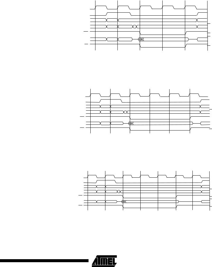
When the SRE bit is set (one), the external memory interface is enabled and the pin functions AD0 - 7 (Port A), A8 - 15 (Port C), ALE (Port E), WR and RD (Port D) are activated as the alternate pin functions. The SRE bit overrides any pin direction settings in the respective data direction registers. See Figure 51 through Figure 54 for a description of the external memory pin functions. When the SRE bit is cleared (zero), the external data memory interface is disabled and the normal pin and data direction settings are used
• Bits 6..4 EMCUCR – SRL2, SRL1, SRL0: Wait State Page Limit
It is possible to configure different wait states for different external memory addresses. The external memory address space can be divided into two pages with different wait state bits. The SRL2, SRL1 and SRL0 bits select the split of the pages (see Table 28 and Figure 50). As defaults, the SRL2, SRL1 and SRL0 bits are set to zero and the entire external memory address space is treated as one page. When the entire SRAM address space is configured as one page, the wait states are configured by the SRW11 and SRW10 bits.
•Bit 1 EMCUCR and Bit 6 MCUCR – SRW11, SRW10: Wait State Select Bits for Upper Page
The SRW11 and SRW10 bits control the number of wait states for the upper page of the external memory address space (see Table 27). Note that if the SRL2, SRL1, and SRL0 bits are set to zero, the SRW11 and SRW10 bit settings will define the wait state of the entire SRAM address space.
82 ATmega161(L)
1228B–09/01

 ATmega161(L)
• Bits 3..2 EMCUCR – SRW01, SRW00: Wait State Select Bits for Lower Page
The SRW01 and SRW00 bits control the number of wait states for the lower page of the external memory address space (see Table 27).
Table 27. Wait States(1)
SRWn1 |
SRWn0 |
Wait States |
|
|
|
0 |
0 |
No wait states |
|
|
|
0 |
1 |
Wait one cycle during read/write strobe |
|
|
|
1 |
0 |
Wait two cycles during read/write strobe |
|
|
|
1 |
1 |
Wait two cycles during read/write and wait one cycle before driving |
|
|
out new address |
|
|
|
Note: 1. |
n = 0 or 1 (lower/upper page) |
|
For further details of the timing and wait states of the external memory interface, see
Figure 51 through Figure 54 for how the setting of the SRW bits affects the timing.
Table 28. Page Limits with Different Settings of SRL2..0
SRL2 |
SRL1 |
SRL0 |
Page Limits |
|
|
|
|
|
|
0 |
0 |
0 |
Lower page = N/A |
|
Upper page = $0460-$FFFF |
||||
|
|
|
||
|
|
|
|
|
0 |
0 |
1 |
Lower page = $0460-$1FFF |
|
Upper page = $2000-$FFFF |
||||
|
|
|
||
|
|
|
|
|
0 |
1 |
0 |
Lower page = $0460-$4FFF |
|
Upper page = $4000-$FFFF |
||||
|
|
|
||
|
|
|
|
|
0 |
1 |
1 |
Lower page = $0460-$5FFF |
|
Upper page = $6000-$FFFF |
||||
|
|
|
||
|
|
|
|
|
1 |
0 |
0 |
Lower page = $0460-$7FFF |
|
Upper page = $8000-$FFFF |
||||
|
|
|
||
|
|
|
|
|
1 |
0 |
1 |
Lower page = $0460-$9FFF |
|
Upper page = $A000-$FFFF |
||||
|
|
|
||
|
|
|
|
|
1 |
1 |
0 |
Lower page = $0460-$BFFF |
|
Upper page = $C000-$FFFF |
||||
|
|
|
||
|
|
|
|
|
1 |
1 |
1 |
Lower page = $0460-$DFFF |
|
Upper page = $E000-$FFFF |
||||
|
|
|
||
|
|
|
|
83
1228B–09/01
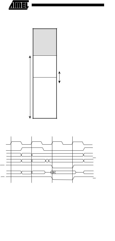
Figure 50. External Memory with Page Select
Data Memory
$0000
Internal memory
$0460
Lower page
SRW01
SRW00
SRL[2..0]
External Memory |
Upper page |
|
(0-63K x 8) |
||
|
SRW11
SRW10
$FFFF
Figure 51. External Data Memory Cycles without Wait State (SRWn1 = 0 and SRWn0 =0)(1)
|
T1 |
|
T2 |
T3 |
T4 |
System Clock Ø |
|
|
|
|
|
ALE |
|
|
|
|
|
Address [15..8] |
Prev. addr. |
XX |
|
Address |
XX |
Data/Address [7..0] |
Prev. data |
XX |
Address XX |
Data |
XX |
WR |
|
|
|
|
|
Data/Address [7..0] |
Prev. data |
XX |
Address |
Data |
XX |
RD |
|
|
|
|
|
 Read Write
Note: 1. SRWn1 = SRW11 (upper page) or SRW01 (lower page), SRWn0 = SRW10 (upper page) or SRW00 (lower page).
The ALE pulse in period T4 is only present if the next instruction accesses the RAM (internal or external). The Data and Address will only change in T4 if ALE is present (the next instruction accesses the RAM).
84 ATmega161(L) 
1228B–09/01
 ATmega161(L)
Figure 52. External Data Memory Cycles with SRWn1 = 0 and SRWn0 = 1(1)
T1 T2 T3 T4 T5
System Clock Ø |
|
|
|
|
|
ALE |
|
|
|
|
|
Address [15..8] |
Prev. addr. |
XX |
|
Address |
XX |
Data/Address [7..0] |
Prev. data |
XX |
Address XX |
Data |
XX |
WR |
|
|
|
|
|
Data/Address [7..0] |
Prev. data |
XX |
Address |
Data |
XX |
RD |
|
|
|
|
|
 Read Write
Note: 1. SRWn1 = SRW11 (upper page) or SRW01 (lower page), SRWn0 = SRW10 (upper page) or SRW00 (lower page). The ALE pulse in period T5 is only present if the next instruction accesses the RAM (internal or external). The Data and Address will only change in T5 if ALE is present (the next instruction accesses the RAM).
Figure 53. External Data Memory Cycles with SRWn1 = 1 and SRWn0 = 0(1)
T1 T2 T3 T4 T5 T6
System Clock Ø |
|
|
|
|
|
ALE |
|
|
|
|
|
Address [15..8] |
Prev. addr. |
XX |
|
Address |
XX |
Data/Address [7..0] |
Prev. data |
XX |
Address XX |
Data |
XX |
WR |
|
|
|
|
|
Data/Address [7..0] |
Prev. data |
XX |
Address |
Data |
XX |
RD |
|
|
|
|
|
 Read Write
Note: 1. SRWn1 = SRW11 (upper page) or SRW01 (lower page), SRWn0 = SRW10 (upper page) or SRW00 (lower page). The ALE pulse in period T6 is only present if the next instruction accesses the RAM (internal or external). The Data and Address will only change in T6 if ALE is present (the next instruction accesses the RAM).
Figure 54. External Data Memory Cycles with SRWn1 = 1 and SRWn0 = 1(1)
T1 T2 T3 T4 T5 T6 T7
System Clock Ø |
|
|
|
|
|
ALE |
|
|
|
|
|
Address [15..8] |
Prev. addr. |
XX |
|
Address |
XX |
Data/Address [7..0] |
Prev. data |
XX |
Address XX |
Data |
XX |
WR |
|
|
|
|
|
Data/Address [7..0] |
Prev. data |
XX |
Address |
Data |
XX |
RD |
|
|
|
|
|
 Read Write
Note: 1. SRWn1 = SRW11 (upper page) or SRW01 (lower page), SRWn0 = SRW10 (upper page) or SRW00 (lower page). The ALE pulse in period T7 is only present if the next instruction accesses the RAM (internal or external). The Data and Address will only change in T7 if ALE is present (the next instruction accesses the RAM).
85
1228B–09/01