Материал: DOC1228

UART0 and UART1 High Byte
Baud Rate Register UBRRHI
|
|
|
|
|
|
|
|
|
|
|
|
|
|
|
|
|
|
|
|
|
|
|
|
|
|
|
|
|
|
|
|
|
|
|
|
|
|
|
|
|
|
|
|
|
|
|
|
|
|
|
|
|
|
|
|
Bit |
7 |
6 |
|
5 |
|
4 |
3 |
2 |
1 |
0 |
|
||
|
|
|
|
|
|
|
|
|
|
|
|
|
|
$20 ($40) |
MSB1 |
|
|
|
|
|
|
LSB1 |
MSB0 |
|
|
LSB0 |
UBRRHI |
|
|
|
|
|
|
|
|
|
|
|
|
||
Read/Write |
R/W |
R/W |
R/W |
R/W |
R/W |
R/W |
R/W |
R/W |
|
||||
Initial Value |
0 |
0 |
|
0 |
|
0 |
0 |
0 |
0 |
0 |
|
||
The UART baud register is a 12-bit register. The four most significant bits are located in a separate register, UBRRHI. Note that both UART0 and UART1 share this register. Bit 7 to bit 4 of UBRRHI contain the four most significant bits of the UART1 baud register. Bit 3 to bit 0 contain the four most significant bits of the UART0 baud register.
UART0 Baud Rate Register
Low Byte – UBRR0
UART1 Baud Rate Register
Low Byte – UBRR1
Bit |
7 |
6 |
5 |
4 |
3 |
2 |
1 |
0 |
|
$09 ($29) |
MSB |
|
|
|
|
|
|
LSB |
UBRR0 |
|
|
|
|
|
|
|
|
|
|
Read/Write |
R/W |
R/W |
R/W |
R/W |
R/W |
R/W |
R/W |
R/W |
|
Initial Value |
0 |
0 |
0 |
0 |
0 |
0 |
0 |
0 |
|
Bit |
7 |
6 |
5 |
4 |
3 |
2 |
1 |
0 |
|
|
|
|
|
|
|
|
|
|
|
$00 ($20) |
MSB |
|
|
|
|
|
|
LSB |
UBRR1 |
|
|
|
|
|
|
|
|
|
|
Read/Write |
R/W |
R/W |
R/W |
R/W |
R/W |
R/W |
R/W |
R/W |
|
Initial Value |
0 |
0 |
0 |
0 |
0 |
0 |
0 |
0 |
|
UBRRn stores the eight least significant bits of the UART baud rate register.
76 ATmega161(L)
1228B–09/01
 ATmega161(L)
Double-speed
Transmission
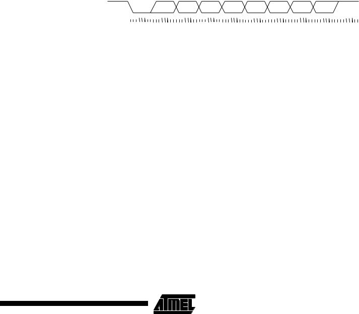
The ATmega161 provides a separate UART mode that allows the user to double the communication speed. By setting the U2X bit in UART Control and Status Register UCSRnA, the UART speed will be doubled. The data reception will differ slightly from normal mode. Since the speed is doubled, the receiver front-end logic samples the signals on RXDn pin at a frequency 8 times the baud rate. While the line is idle, one single sample of logical “0” will be interpreted as the falling edge of a start bit, and the start bit detection sequence is initiated. Let sample 1 denote the first zero-sample. Following the 1-to-0 transition, the receiver samples the RXDn pin at samples 4, 5 and 6. If two or more of these three samples are found to be logical “1”s, the start bit is rejected as a noise spike and the receiver starts looking for the next 1-to-0 transition.
If, however, a valid start bit is detected, sampling of the data bits following the start bit is performed. These bits are also sampled at samples 4, 5 and 6. The logical value found in at least two of the three samples is taken as the bit value. All bits are shifted into the transmitter shift register as they are sampled. Sampling of an incoming character is shown in Figure 48.
Figure 48. Sampling Received Data when the Transmission Speed is Doubled
RXD
START BIT |
D0 |
D1 |
D2 |
D3 |
D4 |
D5 |
D6 |
D7 |
STOP BIT |
RECEIVER
SAMPLING
The Baud Rate Generator in |
Note that the baud rate equation is different from the equation on page 75 when the |
Double UART Speed Mode |
UART speed is doubled: |
|
fCK |
|
BAUD = 8(UBR------------------------------+ 1 ) |
|
• BAUD = Baud rate |
|
• fCK= Crystal Clock frequency |
|
• UBR = Contents of the UBRRHI and UBRR registers (0 - 4095) |
|
• Note that this equation is only valid when the UART transmission speed is doubled. |
|
For standard crystal frequencies, the most commonly used baud rates can be generated |
|
by using the UBR settings in Table 24. UBR values that yield an actual baud rate differ- |
|
ing less than 1.5% from the target baud rate are boldface in the table. However, since |
|
the number of samples are reduced and the system clock might have some variance |
|
(this applies especially when using resonators), it is recommended that the baud rate |
|
error be less than 0.5%. |
77
1228B–09/01
Table 25. UBR Settings at Various Crystal Frequencies in Double-speed Mode
Baud Rate |
1.0000 MHz |
% Error |
1.8432 MHz |
% Error |
2.0000 MHz |
% Error |
|
|
|
|
|
|
|
2400 |
UBR = 51 |
0.2 |
UBR = 95 |
0.0 |
UBR = 103 |
0.2 |
4800 |
UBR = 25 |
0.2 |
UBR = 47 |
0.0 |
UBR = 51 |
0.2 |
9600 |
UBR = 12 |
0.2 |
UBR = 23 |
0.0 |
UBR = 25 |
0.2 |
14400 |
UBR = 8 |
3.7 |
UBR = 15 |
0.0 |
UBR = 16 |
2.1 |
19200 |
UBR = 6 |
7.5 |
UBR = 11 |
0.0 |
UBR = 12 |
0.2 |
28800 |
UBR = 3 |
7.8 |
UBR = 7 |
0.0 |
UBR = 8 |
3.7 |
38400 |
UBR = 2 |
7.8 |
UBR = 5 |
0.0 |
UBR = 6 |
7.5 |
57600 |
UBR = 1 |
7.8 |
UBR = 3 |
0.0 |
UBR = 3 |
7.8 |
76800 |
UBR = 1 |
22.9 |
UBR = 2 |
0.0 |
UBR = 2 |
7.8 |
115200 |
UBR = 0 |
84.3 |
UBR = 1 |
0.0 |
UBR = 1 |
7.8 |
230400 |
- |
- |
UBR = 0 |
0.0 |
UBR = 0 |
84.3 |
|
|
|
|
|
|
|
Baud Rate |
3.2768 MHz |
% Error |
3.6864 MHz |
% Error |
4.0000 MHz |
% Error |
|
|
|
|
|
|
|
2400 |
UBR = 170 |
0.2 |
UBR = 191 |
0.0 |
UBR = 207 |
0.2 |
4800 |
UBR = 84 |
0.4 |
UBR = 95 |
0.0 |
UBR = 103 |
0.2 |
9600 |
UBR = 42 |
0.8 |
UBR = 47 |
0.0 |
UBR = 51 |
0.2 |
14400 |
UBR = 27 |
1.6 |
UBR = 31 |
0.0 |
UBR = 34 |
0.8 |
19200 |
UBR = 20 |
1.6 |
UBR = 23 |
0.0 |
UBR = 25 |
0.2 |
28800 |
UBR = 13 |
1.6 |
UBR = 15 |
0.0 |
UBR = 16 |
2.1 |
38400 |
UBR = 10 |
3.1 |
UBR = 11 |
0.0 |
UBR = 12 |
0.2 |
57600 |
UBR = 6 |
1.6 |
UBR = 7 |
0.0 |
UBR = 8 |
3.7 |
76800 |
UBR = 4 |
6.2 |
UBR = 5 |
0.0 |
UBR = 6 |
7.5 |
115200 |
UBR = 3 |
12.5 |
UBR = 3 |
0.0 |
UBR = 3 |
7.8 |
230400 |
UBR = 1 |
12.5 |
UBR = 1 |
0.0 |
UBR = 1 |
7.8 |
460800 |
UBR = 0 |
12.5 |
UBR = 0 |
0.0 |
UBR = 0 |
7.8 |
912600 |
- |
- |
- |
- |
UBR = 0 |
84.3 |
|
|
|
|
|
|
|
Baud Rate |
7.3728 MHz |
% Error |
8.0000 MHz |
% Error |
9.2160 MHz |
% Error |
|
|
|
|
|
|
|
2400 |
UBR = 383 |
0.0 |
UBR = 416 |
0.1 |
UBR = 479 |
0.0 |
4800 |
UBR = 191 |
0.0 |
UBR = 207 |
0.2 |
UBR = 239 |
0.0 |
9600 |
UBR = 95 |
0.0 |
UBR = 103 |
0.2 |
UBR = 119 |
0.0 |
14400 |
UBR = 63 |
0.0 |
UBR = 68 |
0.6 |
UBR = 79 |
0.0 |
19200 |
UBR = 47 |
0.0 |
UBR = 51 |
0.2 |
UBR = 59 |
0.0 |
28800 |
UBR = 31 |
0.0 |
UBR = 34 |
0.8 |
UBR = 39 |
0.0 |
38400 |
UBR = 23 |
0.0 |
UBR = 25 |
0.2 |
UBR = 29 |
0.0 |
57600 |
UBR = 15 |
0.0 |
UBR = 16 |
2.1 |
UBR = 19 |
0.0 |
76800 |
UBR = 11 |
0.0 |
UBR = 12 |
0.2 |
UBR = 14 |
0.0 |
115200 |
UBR = 7 |
0.0 |
UBR = 8 |
3.7 |
UBR = 9 |
0.0 |
230400 |
UBR = 3 |
0.0 |
UBR = 3 |
7.8 |
UBR = 4 |
0.0 |
460800 |
UBR = 1 |
0.0 |
UBR = 1 |
7.8 |
UBR = 2 |
20.0 |
912600 |
UBR = 0 |
0.0 |
UBR = 0 |
7.8 |
UBR = 0 |
20.0 |
|
|
|
|
|
|
|
78 ATmega161(L)
1228B–09/01
Analog Comparator
Analog Comparator Control
and Status Register – ACSR
1228B–09/01
ATmega161(L)
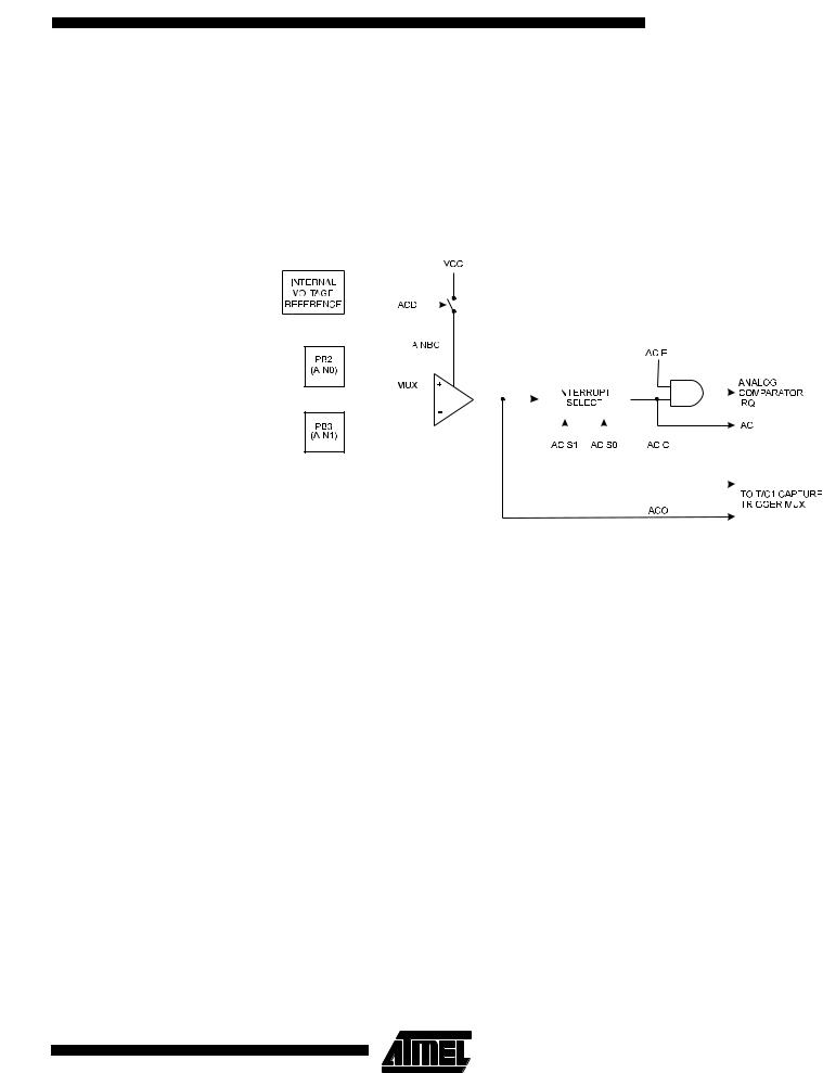
The Analog Comparator compares the input values on the positive input PB2 (AIN0) and negative input PB3 (AIN1). When the voltage on the positive input PB2 (AIN0) is higher than the voltage on the negative input PB3 (AIN1), the Analog Comparator Output (ACO) is set (one). The comparator’s output can be set to trigger the Timer/Counter1 Input Capture function. In addition, the comparator can trigger a separate interrupt, exclusive to the Analog Comparator. The user can select interrupt triggering on comparator output rise, fall or toggle. A block diagram of the comparator and its surrounding logic is shown in Figure 49.
Figure 49. Analog Comparator Block Diagram
|
|
|
|
|
|
|
|
|
|
|
|
|
|
|
|
|
|
|
|
|
|
|
|
|
|
|
|
|
|
|
|
|
|
|
|
|
|
|
|
|
|
|
|
|
|
|
|
|
|
|
|
|
|
|
|
|
|
|
|
|
|
|
|
|
|
|
|
|
|
|
|
|
|
|
|
|
|
|
|
|
|
|
|
|
|
|
|
|
|
|
|
|
|
|
|
|
|
|
|
|
|
|
|
|
|
|
|
|
|
|
|
|
|
|
|
|
|
|
|
|
|
|
|
|
|
|
|
|
|
|
|
|
|
|
|
|
|
|
|
|
|
|
|
|
|
|
|
|
|
|
|
|
|
|
|
|
|
|
|
|
|
|
|
|
|
|
|
|
|
|
|
|
|
|
|
|
|
|
|
|
|
|
|
|
|
|
|
|
|
|
|
|
|
|
|
|
|
|
|
|
|
|
|
|
|
|
|
|
|
|
|
|
|
|
|
|
|
|
|
|
|
|
|
|
|
|
|
|
|
|
|
|
|
|
|
|
|
|
|
|
|
|
|
|
|
|
|
|
|
|
|
|
|
|
|
|
|
|
|
|
|
|
|
|
|
|
|
|
|
|
|
|
|
|
|
|
|
|
|
|
|
|
|
|
|
|
|
|
|
|
|
|
|
|
|
|
|
|
|
|
|
|
|
|
|
|
|
|
|
|
|
|
|
|
|
|
|
|
|
|
|
|
|
|
|
|
|
|
|
|
|
|
|
|
|
|
|
|
|
|
|
|
|
|
|
|
|
|
|
|
|
|
|
|
|
|
|
|
|
|
|
|
|
|
|
|
|
|
|
|
|
|
|
|
|
|
|
|
|
|
|
|
|
|
|
|
|
|
|
|
|
|
|
|
|
|
|
|
|
|
|
|
|
|
|
|
|
|
|
|
|
|
|
|
|
|
|
|
|
|
|
|
|
|
|
|
|
|
|
|
|
|
|
|
|
|
|
|
|
|
|
|
|
|
|
|
|
|
|
|
|
|
|
|
|
|
|
|
|
|
|
|
|
|
|
|
|
|
|
|
|
|
|
|
|
|
|
|
|
|
|
|
|
|
|
|
|
|
|
|
|
|
|
|
|
|
|
|
|
|
|
|
|
|
|
|
|
|
|
|
|
|
|
|
|
|
|
|
|
|
|
|
|
|
|
|
|
|
|
|
|
|
|
|
|
|
|
|
|
|
|
|
|
|
|
|
|
|
|
|
|
|
|
|
|
|
|
|
|
|
|
|
|
|
|
|
|
|
|
|
|
|
|
|
|
|
|
|
|
|
|
|
|
|
|
|
|
|
|
|
|
|
|
|
|
|
|
|
|
|
|
|
|
|
|
|
|
|
|
|
|
|
|
|
|
|
|
|
|
|
|
|
|
|
|
|
|
|
|
Bit |
7 |
|
|
6 |
|
|
5 |
4 |
|
|
3 |
|
2 |
|
|
1 |
|
0 |
|
|
|||||||||
|
|
|
|
|
|
|
|
|
|
|
|
||||||||||||||||||
|
|
|
|
|
|
|
|
|
|
|
|
||||||||||||||||||
|
|
|
|
|
|
|
|
|
|
|
|
|
|
|
|
|
|
|
|
|
|
|
|
|
|
|
|
|
|
$08 ($28) |
ACD |
|
AINBG |
ACO |
ACI |
|
ACIE |
ACIC |
ACIS1 |
|
ACIS0 |
ACSR |
|||||||||||||||||
|
|
|
|
|
|
|
|
|
|
|
|
|
|
|
|
|
|
|
|
|
|
|
|
|
|
|
|
|
|
Read/Write |
R/W |
|
R/W |
|
R |
R/W |
|
R/W |
|
R/W |
R/W |
|
|
R/W |
|
||||||||||||||
Initial Value |
0 |
|
|
0 |
|
|
N/A |
0 |
|
|
0 |
|
0 |
|
|
0 |
|
0 |
|
|
|||||||||
• Bit 7 – ACD: Analog Comparator Disable
When this bit is set (one), the power to the Analog Comparator is switched off. This bit can be set at any time to turn off the Analog Comparator. This will reduce power consumption in active and idle mode. When changing the ACD bit, the Analog Comparator Interrupt must be disabled by clearing the ACIE bit in ACSR. Otherwise, an interrupt can occur when the bit is changed.
• Bit 6 – AINBG: Analog Comparator Bandgap Select
When this bit is set, a fixed bandgap voltage of 1.22 ± 0.05V replaces the normal input to the positive input (AIN0) of the comparator. When this bit is cleared, the normal input pin PB2 is applied to the positive input of the comparator.
• Bit 5 – ACO: Analog Comparator Output
ACO is directly connected to the comparator output.
79
• Bit 4 – ACI: Analog Comparator Interrupt Flag
This bit is set (one) when a comparator output event triggers the interrupt mode defined by ACI1 and ACI0. The Analog Comparator Interrupt routine is executed if the ACIE bit is set (one) and the I-bit in SREG is set (one). ACI is cleared by hardware when executing the corresponding interrupt handling vector. Alternatively, ACI is cleared by writing a logical “1” to the flag.
• Bit 3 – ACIE: Analog Comparator Interrupt Enable
When the ACIE bit is set (one) and the I-bit in the Status Register is set (one), the Analog Comparator Interrupt is enabled. When cleared (zero), the interrupt is disabled.
• Bit 2 – ACIC: Analog Comparator Input Capture Enable
When set (one), this bit enables the Input Capture function in Timer/Counter1 to be triggered by the Analog Comparator. The comparator output is, in this case, directly connected to the Input Capture front-end logic, making the comparator utilize the noise canceler and edge select features of the Timer/Counter1 Input Capture Interrupt. When cleared (zero), no connection between the Analog Comparator and the Input Capture function is given. To make the comparator trigger the Timer/Counter1 Input Capture Interrupt, the TICIE1 bit in the Timer Interrupt Mask Register (TIMSK) must be set (one).
• Bits 1, 0 – ACIS1, ACIS0: Analog Comparator Interrupt Mode Select
These bits determine which comparator events trigger the Analog Comparator Interrupt.
The different settings are shown in Table 26.
Table 26. |
ACIS1/ACIS0 Settings(1) |
||
ACIS1 |
|
ACIS0 |
Interrupt Mode |
|
|
|
|
0 |
|
0 |
Comparator Interrupt on Output Toggle |
|
|
|
|
0 |
|
1 |
Reserved |
|
|
|
|
1 |
|
0 |
Comparator Interrupt on Falling Output Edge |
|
|
|
|
1 |
|
1 |
Comparator Interrupt on Rising Output Edge |
|
|
|
|
Note: 1. When changing the ACIS1/ACIS0 bits, the Analog Comparator Interrupt must be disabled by clearing its Interrupt Enable bit in the ACSR register. Otherwise, an interrupt can occur when the bits are changed.
Caution: Using the SBI or CBI instruction on bits other than ACI in this register will write a one back into ACI if it is read as set, thus clearing the flag.
The Analog Comparator pins (PB2 and PB3) are also used as the TXD1 and RXD1 pins for UART1. Note that if the UART1 transceiver or receiver is enabled, the UART1 will override the settings in the DDRB register even if the Analog Comparator is enabled. Therefore, it is not recommended to use UART1 if the Analog Comparator is needed in the same application at the same time. See “UARTs” on page 68 for more details.
80 ATmega161(L)
1228B–09/01