Материал: DOC1228

SPI Control Register – SPCR
Bit |
7 |
6 |
5 |
4 |
3 |
2 |
1 |
0 |
|
|
|
|
|
|
|
|
|
|
|
$0D ($2D) |
SPIE |
SPE |
DORD |
MSTR |
CPOL |
CPHA |
SPR1 |
SPR0 |
SPCR |
|
|
|
|
|
|
|
|
|
|
Read/Write |
R/W |
R/W |
R/W |
R/W |
R/W |
R/W |
R/W |
R/W |
|
Initial Value |
0 |
0 |
0 |
0 |
0 |
0 |
0 |
0 |
|
• Bit 7 – SPIE: SPI Interrupt Enable
This bit causes the SPI interrupt to be executed if SPIF bit in the SPSR register is set and if the global interrupt enable bit in SREG is set.
• Bit 6 – SPE: SPI Enable
When the SPE bit is set (one), the SPI is enabled. This bit must be set to enable any SPI operations.
• Bit 5 – DORD: Data Order
When the DORD bit is set (one), the LSB of the data word is transmitted first.
When the DORD bit is cleared (zero), the MSB of the data word is transmitted first.
• Bit 4 – MSTR: Master/Slave Select
This bit selects Master SPI mode when set (one), and Slave SPI mode when cleared (zero). If SS is configured as an input and is driven low while MSTR is set, MSTR will be cleared and SPIF in SPSR will become set. The user will then have to set MSTR to reenable SPI master mode.
• Bit 3 – CPOL: Clock Polarity
When this bit is set (one), SCK is high when idle. When CPOL is cleared (zero), SCK is low when idle. Refer to Figure 43 and Figure 44 for additional information.
• Bit 2 – CPHA: Clock Phase
Refer to Figure 43 or Figure 44 for the functionality of this bit.
• Bits 1, 0 – SPR1, SPR0: SPI Clock Rate Select 1 and 0
These two bits control the SCK rate of the device configured as a master. SPR1 and
SPR0 have no effect on the slave. The relationship between SCK and the Oscillator
Clock frequency (fcl) is shown in Table 23:
Table 23. Relationship between SCK and the Oscillator Frequency(1)
SPI2X |
SPR1 |
SPR0 |
SCK Frequency |
|
|
|
|
0 |
0 |
0 |
fcl/4 |
0 |
0 |
1 |
fcl/16 |
0 |
1 |
0 |
fcl/64 |
0 |
1 |
1 |
fcl/128 |
1 |
0 |
0 |
fcl/2 |
1 |
0 |
1 |
fcl/8 |
1 |
1 |
0 |
fcl/32 |
1 |
1 |
1 |
fcl/64 |
Note: 1. When the SPI is configured as slave, the SPI is only guaranteed to work at fcl/4.
66 ATmega161(L)
1228B–09/01

ATmega161(L)
SPI Status Register – SPSR
Bit |
7 |
6 |
5 |
4 |
3 |
2 |
1 |
0 |
|
$0E ($2E) |
SPIF |
WCOL |
– |
– |
– |
– |
– |
SPI2X |
SPSR |
|
|
|
|
|
|
|
|
|
|
Read/Write |
R |
R |
R |
R |
R |
R |
R |
R/W |
|
Initial Value |
0 |
0 |
0 |
0 |
0 |
0 |
0 |
0 |
|
• Bit 7 – SPIF: SPI Interrupt Flag
When a serial transfer is complete, the SPIF bit is set (one) and an interrupt is generated if SPIE in SPCR is set (one) and global interrupts are enabled. If SS is an input and is driven low when the SPI is in master mode, this will also set the SPIF flag. SPIF is cleared by hardware when executing the corresponding interrupt handling vector. Alternatively, the SPIF bit is cleared by first reading the SPI status register with SPIF set (one), then by accessing the SPI Data Register (SPDR).
• Bit 6 – WCOL: Write Collision Flag
The WCOL bit is set if the SPI Data Register (SPDR) is written during a data transfer. The WCOL bit (and the SPIF bit) are cleared (zero) by first reading the SPI Status Register with WCOL set (one), and then by accessing the SPI Data Register.
• Bits 5..1 – Res: Reserved Bits
These bits are reserved bits in the ATmega161 and will always read as zero.
• Bit 0 – SPI2X: Double SPI Speed Bit
When this bit is set (one), the SPI speed (SCK frequency) will be doubled when the SPI is in master mode (see Table 23). This means that the maximum SCK period will be two CPU clock periods. When the SPI is configured as slave, the SPI is only guaranteed to work at fcl/4.
The SPI interface on the ATmega161 is also used for program memory and EEPROM downloading or uploading. See page 123 for serial programming and verification.
SPI Data Register – SPDR
Bit |
7 |
6 |
5 |
4 |
3 |
2 |
1 |
0 |
|
$0F ($2F) |
MSB |
|
|
|
|
|
|
LSB |
SPDR |
|
|
|
|
|
|
|
|
|
|
Read/Write |
R/W |
R/W |
R/W |
R/W |
R/W |
R/W |
R/W |
R/W |
|
Initial Value |
x |
x |
x |
x |
x |
x |
x |
x |
Undefined |
The SPI Data Register is a read/write register used for data transfer between the register file and the SPI Shift Register. Writing to the register initiates data transmission. Reading the register causes the Shift Register Receive buffer to be read.
67
1228B–09/01
UARTs
Data Transmission
The ATmega161 features two full-duplex (separate receive and transmit registers) Universal Asynchronous Receiver and Transmitters (UARTs). The main features are:
•Baud Rate Generator Generates any Baud Rate
•High Baud Rates at low XTAL Frequencies
•8 or 9 Bits Data
•Noise Filtering
•Overrun Detection
•Framing Error Detection
•False Start Bit Detection
•Three Separate Interrupts on TX Complete, TX Data Register Empty, and RX Complete
•Multi-processor Communication Mode
•Double-speed UART Mode
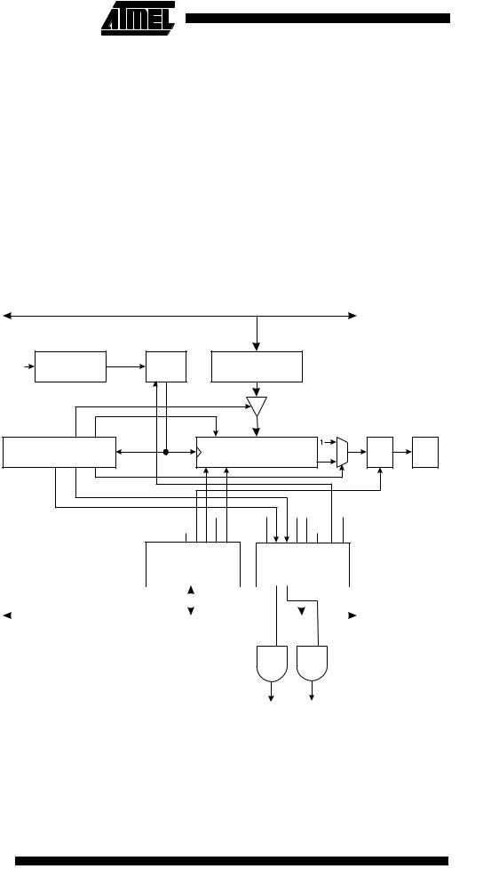
A block schematic of the UART transmitter is shown in Figure 45. The two UARTs are identical and the functionality is described in general for the two UARTs.
Figure 45. |
UART Transmitter |
|
|
|
|
|
|
|
|
|
|
||
|
|
|
|
DATA BUS |
|
|
|
|
|
|
|
||
XTAL |
BAUD RATE |
BAUD x 16 |
/16 |
|
|
|
|
UART I/O DATA |
|
|
|
|
|
|
|
|
|
|
|
|
|
|
|||||
GENERATOR |
|
|
|
|
REGISTER (UDRn) |
|
|
|
|
||||
|
|
|
|
|
|
|
|
|
|
||||
|
|
|
STORE UDRn |
|
|
|
|
|
|
|
|
|
|
|
|
|
SHIFT ENABLE |
|
|
|
|
|
|
|
|
PIN CONTROL |
|
|
|
|
|
|
|
|
|
|
|
|
|
|
|
|
|
|
|
|
|
|
|
|
|
|
|
LOGIC |
|
CONTROL LOGIC |
|
BAUD |
|
|
|
10(11)-BIT TX |
|
|
TXDn |
PD1/ |
|||
|
|
|
|
|
SHIFT REGISTER |
|
|
|
PB3 |
||||
|
|
|
|
|
|
|
|
|
|
|
|||
|
|
|
IDLE |
|
|
|
|
|
|
|
|
|
|
|
|
|
|
RXENn |
TXENn |
CHR9n |
RXB8n |
TXB8n |
RXCn TXCn UDREn FEn |
ORn |
U2Xn |
MPCMPn |
|
|
UART CONTROL AND |
UART CONTROL AND |
|||||||||||
|
STATUS REGISTER |
STATUS REGISTER |
|||||||||||
|
|
|
|
(UCSRnB) |
|
(UCSRnA) |
|||||||
|
|
|
|
|
|
|
|
|
|
|
|
|
|
|
RXCIEn |
|
TXCIEn |
UDRIEn |
|
|
DATA BUS |
|
TXCn UDREn |
|
|
||
|
|
||||||||||||
|
|
|
|
|
|
|
|||||||
|
|
|
|
|
|
|
|
|
|
|
|
|
|
|
|
|
|
|
|
|
|
|
|
|
|
|
|
|
|
|
|
|
|
|
|
|
|
|
|
|
|
|
TXCn |
UDREn |
n = 0,1 |
IRQ |
IRQ |
Data transmission is initiated by writing the data to be transmitted to the UART I/O Data Register, UDRn. Data is transferred from UDRn to the Transmit shift register when:
•A new character has been written to UDRn after the stop bit from the previous character has been shifted out. The shift register is loaded immediately.
68 ATmega161(L)
1228B–09/01

 ATmega161(L)
•A new character has been written to UDRn before the stop bit from the previous character has been shifted out. The shift register is loaded when the stop bit of the character currently being transmitted has been shifted out.
If the 10(11)-bit Transmit shift register is empty, data is transferred from UDRn to the shift register. At this time the UDREn (UART Data Register Empty) bit in the UART Control and Status Register, UCSRnA, is set. When this bit is set (one), the UART is ready to receive the next character. At the same time as the data is transferred from UDRn to the 10(11)-bit shift register, bit 0 of the shift register is cleared (start bit) and bit 9 or 10 is set (stop bit). If 9-bit data word is selected (the CHR9n bit in the UART Control and Status Register, UCSRnB, is set), the TXB8 bit in UCSRnB is transferred to bit 9 in the Transmit shift register.
On the baud rate clock following the transfer operation to the shift register, the start bit is shifted out on the TXDn pin. Then follows the data, LSB first. When the stop bit has been shifted out, the shift register is loaded if any new data has been written to the UDRn during the transmission. During loading, UDREn is set. If there is no new data in the UDRn register to send when the stop bit is shifted out, the UDREn flag will remain set until UDRn is written again. When no new data has been written and the stop bit has been present on TXDn for one bit length, the TX Complete flag (TXCn) in UCSRnA is set.
The TXENn bit in UCSRnB enables the UART transmitter when set (one). When this bit is cleared (zero), the PD1 (UART0) or PB3 (UART1) pin can be used for general I/O. When TXENn is set, the UART transmitter will be connected to PD1 (UART0) or PB3 (UART1), which is forced to be an output pin regardless of the setting of the DDD1 bit in DDRD (UART0) or DDB3 in DDRB (UART1). Note that PB3 (UART1) also is used as one of the input pins to the Analog Comparator. It is therefore not recommended to use UART1 if the Analog Comparator is also used in the application at the same time.
69
1228B–09/01
Data Reception
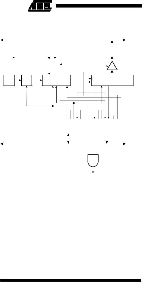
Figure 46 shows a block diagram of the UART receiver.
Figure 46. |
UART Receiver |
|
|
|
|
|
|
|
|
|
|
|
|
|
|
|
|
||||||||||
|
|
|
|
|
|
|
|
|
|
|
|
|
|
|
DATA BUS |
|
|
||||||||||
|
|
|
|
|
|
|
|
|
|
|
|
|
|
|
|
|
|
|
|
|
|
|
|
|
|
|
|
|
|
|
|
|
|
|
|
|
|
|
|
|
|
|
|
|
|
|
|
|
|
|
|
|
|
|
|
|
|
|
|
|
|
|
|
|
|
|
|
|
|
|
|
|
|
|
|
|
|
|
UART I/O DATA |
|
|||
|
|
|
|
|
|
|
|
|
|
|
|
BAUD x 16 |
|
|
|
BAUD |
REGISTER (UDRn) |
|
|||||||||
XTAL |
|
|
|
BAUD RATE |
/16 |
|
|
||||||||||||||||||||
|
|
|
|
|
|
|
|
||||||||||||||||||||
|
|
|
|
|
|||||||||||||||||||||||
|
|
|
GENERATOR |
|
|
|
|
|
|
|
|
|
|
|
|
|
|
||||||||||
|
|
|
|
|
|
|
|
|
|
|
|
|
|
|
|
|
|
|
|
|
|
||||||
|
|
|
|
|
|
|
|
|
|
|
|
|
|
|
|
|
|
STORE UDRn |
|
|
|
|
|
|
|
|
|
|
|
|
|
|
|
|
|
|
|
|
|
|
|
|
|
|
|
|
|
|
|
|
|||||
|
|
|
|
|
|
PIN CONTROL |
|
|
|
|
|
|
|
|
|
|
|
|
|
|
|
|
|||||
|
|
|
|
|
|
|
|
LOGIC |
|
|
|
|
|
|
|
|
|
|
|
|
|
|
|
|
|||
|
|
|
|
|
|
|
|
|
|
|
|
|
|
|
|
|
|
|
|
|
|
|
|
||||
|
|
|
|
|
|
|
|
|
|
|
|
|
|
|
|
|
|
|
|
|
|
|
|
|
|
|
|
|
|
PD0/ |
|
|
|
|
|
|
RXDn |
DATA RECOVERY |
|
|
|
|
|
10(11)-BIT RX |
|
||||||||||
|
|
|
|
|
|
|
|
|
|||||||||||||||||||
|
|
PB2 |
|
|
|
|
|
|
|
|
|
LOGIC |
|
|
|
|
|
SHIFT REGISTER |
|
||||||||
|
|
|
|
|
|
|
|
|
|
|
|
|
|
|
|||||||||||||
RXENn |
TXENn |
CHR9n |
RXB8n |
TXB8n |
RXCn |
TXCn |
UDREn |
FEn |
ORn |
U2Xn |
MPCMPn |
|
UART CONTROL AND |
|
UART CONTROL AND |
|||||||||
|
STATUS REGISTER |
|
STATUS REGISTER |
|||||||||
|
|
|
|
(UCSRnB) |
|
|
(UCSRnA) |
|||||
|
|
|
|
|
|
|
|
|
|
|
|
|
|
RXCIEn |
TXCIEn |
|
UDRIEn |
|
|
|
DATA BUS |
TXCn |
|
|
|
|
|
|
|
|||||||||
|
|
|
|
|
|
|
||||||
|
|
|
|
|
|
|
|
|
|
|
|
|
|
|
|
|
|
|
|
|
|
|
|
|
|
n = 0,1 |
RXCn |
IRQ |
The receiver front-end logic samples the signal on the RXDn pin at a frequency 16 times the baud rate. While the line is idle, one single sample of logical “0” will be interpreted as the falling edge of a start bit, and the start bit detection sequence is initiated. Let sample 1 denote the first zero-sample. Following the 1-to-0 transition, the receiver samples the RXDn pin at samples 8, 9 and 10. If two or more of these three samples are found to be logical “1”s, the start bit is rejected as a noise spike and the receiver starts looking for the next 1-to-0 transition.
If, however, a valid start bit is detected, sampling of the data bits following the start bit is performed. These bits are also sampled at samples 8, 9 and 10. The logical value found in at least two of the three samples is taken as the bit value. All bits are shifted into the transmitter shift register as they are sampled. Sampling of an incoming character is shown in Figure 47. Note that the description above is not valid when the UART transmission speed is doubled. See “Double-speed Transmission” on page 77 for a detailed description.
70 ATmega161(L)
1228B–09/01