Материал: DOC1228

EEPROM Control Register –
EECR
1228B–09/01
ATmega161(L)
Bit |
7 |
6 |
5 |
4 |
3 |
2 |
1 |
0 |
|
$1C ($3C) |
– |
– |
– |
– |
EERIE |
EEMWE |
EEWE |
EERE |
EECR |
|
|
|
|
|
|
|
|
|
|
Read/Write |
R |
R |
R |
R |
R/W |
R/W |
R/W |
R/W |
|
Initial Value |
0 |
0 |
0 |
0 |
0 |
0 |
X |
0 |
|
• Bits 7..4 – Res: Reserved Bits
These bits are reserved bits in the ATmega161 and will always read as zero.
• Bit 3 – EERIE: EEPROM Ready Interrupt Enable
When the I-bit in SREG and EERIE are set (one), the EEPROM Ready Interrupt is enabled. When cleared (zero), the interrupt is disabled. The EEPROM Ready interrupt generates a constant interrupt when EEWE is cleared (zero).
• Bit 2 – EEMWE: EEPROM Master Write Enable
The EEMWE bit determines whether setting EEWE to one causes the EEPROM to be written. When EEMWE is set (one), setting EEWE will write data to the EEPROM at the selected address. If EEMWE is zero, setting EEWE will have no effect. When EEMWE has been set (one) by software, hardware clears the bit to zero after four clock cycles. See the description of the EEWE bit for an EEPROM write procedure.
• Bit 1 – EEWE: EEPROM Write Enable
The EEPROM Write Enable Signal (EEWE) is the write strobe to the EEPROM. When address and data are correctly set up, the EEWE bit must be set to write the value into the EEPROM. The EEMWE bit must be set when the logical “1” is written to EEWE, otherwise no EEPROM write takes place. The following procedure should be followed when writing the EEPROM (the order of steps 2 and 3 is not essential):
1.Wait until EEWE becomes zero.
2.Write new EEPROM address to EEAR (optional).
3.Write new EEPROM data to EEDR (optional).
4.Write a logical “1” to the EEMWE bit in EECR (to be able to write a logical “1” to the EEMWE bit, the EEWE bit must be written to zero in the same cycle).
5.Within four clock cycles after setting EEMWE, write a logical “1” to EEWE.
Caution: An interrupt between step 4 and step 5 will make the write cycle fail, since the EEPROM Master Write Enable will time-out. If an interrupt routine accessing the EEPROM is interrupting another EEPROM access, the EEAR or EEDR register will be modified, causing the interrupted EEPROM access to fail. It is recommended to have the global interrupt flag cleared during the four last steps to avoid these problems.
When the write access time has elapsed, the EEWE bit is cleared (zero) by hardware. The user software can poll this bit and wait for a zero before writing the next byte. When EEWE has been set, the CPU is halted for two cycles before the next instruction is executed.
• Bit 0 – EERE: EEPROM Read Enable
The EEPROM Read Enable signal (EERE) is the read strobe to the EEPROM. When the correct address is set up in the EEAR register, the EERE bit must be set. When the EERE bit is cleared (zero) by hardware, requested data is found in the EEDR register. The EEPROM read access takes one instruction and there is no need to poll the EERE bit. When EERE has been set, the CPU is halted for four cycles before the next instruction is executed.
61

Prevent EEPROM
Corruption
The user should poll the EEWE bit before starting the read operation. If a write operation is in progress when new data or address is written to the EEPROM I/O registers, the write operation will be interrupted and the result is undefined.
An RC oscillator is used to time EEPROM write access. The table below lists the typical programming time listed for EEPROM access from CPU.
Table 21. EEPROM Access Time from CPU“See “Typical Characteristics” on page 136 to find RC oscillator frequency.” on page 62(1)
|
No. of RC |
Min Programming |
Max Programming |
Symbol |
Oscillator Cycles |
Time |
Time |
|
|
|
|
EEPROM write (from CPU) |
2048 |
2.0 ms |
3.4 ms |
|
|
|
|
Note: 1. See “Typical Characteristics” on page 136 to find RC oscillator frequency.
During periods of low VCC, the EEPROM data can be corrupted because the supply voltage is too low for the CPU and the EEPROM to operate properly. These issues are the same as for board-level systems using the EEPROM, and the same design solutions should be applied.
An EEPROM data corruption can be caused by two situations when the voltage is too low. First, a regular write sequence to the EEPROM requires a minimum voltage to operate correctly. Secondly, the CPU itself can execute instructions incorrectly if the supply voltage for executing instructions is too low.
EEPROM data corruption can easily be avoided by following these design recommendations (one is sufficient):
1.Keep the AVR RESET active (low) during periods of insufficient power supply voltage. This can be done by enabling the internal Brown-out Detector (BOD) if
the operating voltage matches the detection level. If not, an external low VCC Reset Protection circuit can be applied.
2.Keep the AVR core in Power-down Sleep mode during periods of low VCC. This will prevent the CPU from attempting to decode and execute instructions, effectively protecting the EEPROM registers from unintentional writes.
3.Store constants in Flash memory if the ability to change memory contents from software is not required. Flash memory cannot be updated by the CPU unless the boot loader software supports writing to the Flash and the Boot Lock bits are configured so that writing to the Flash memory from the CPU is allowed. See “Boot Loader Support” on page 108 for details.
62 ATmega161(L)
1228B–09/01
 ATmega161(L)
Serial Peripheral
Interface – SPI
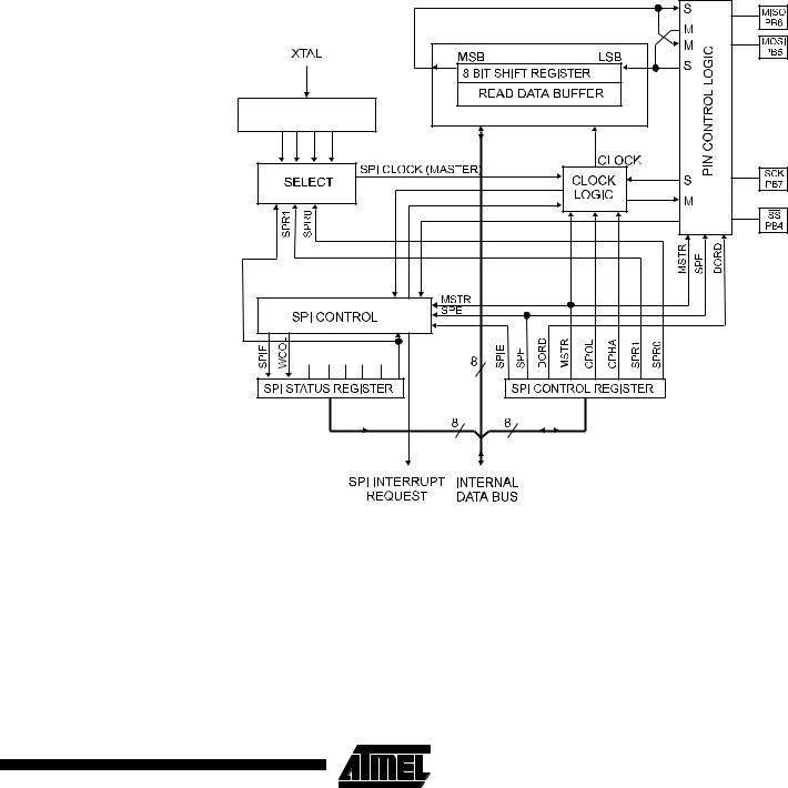
The Serial Peripheral Interface (SPI) allows high-speed synchronous data transfer between the ATmega161 and peripheral devices or between several AVR devices. The ATmega161 SPI features include the following:
•Full-duplex, 3-wire Synchronous Data Transfer
•Master or Slave Operation
•LSB First or MSB First Data Transfer
•Seven Programmable Bit Rates
•End-of-Transmission Interrupt Flag
•Write Collision Flag Protection
•Wake-up from Idle Mode (Slave Mode Only)
•Double-speed (CK/2) Master SPI Mode
Figure 41. SPI Block Diagram
DIVIDER |
/2/4/8/16/32/64/128 |
SPI2X |
SPI2X |
63
1228B–09/01
SS Pin Functionality
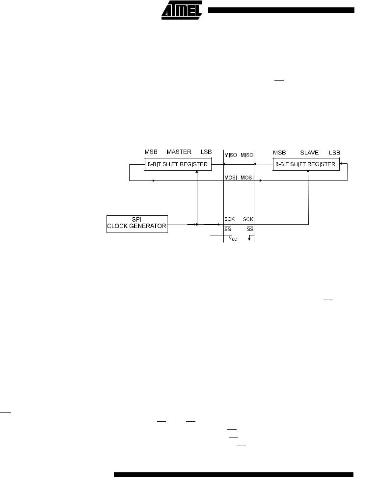
The interconnection between master and slave CPUs with SPI is shown in Figure 42. The PB7(SCK) pin is the clock output in the master mode and is the clock input in the slave mode. Writing to the SPI data register of the master CPU starts the SPI clock generator, and the data written shifts out of the PB5(MOSI) pin and into the PB5(MOSI) pin of the slave CPU. After shifting one byte, the SPI clock generator stops, setting the end- of-transmission flag (SPIF). If the SPI interrupt enable bit (SPIE) in the SPCR register is set, an interrupt is requested. The Slave Select input, PB4(SS), is set low to select an individual slave SPI device. The two shift registers in the master and the slave can be considered as one distributed 16-bit circular shift register. This is shown in Figure 42. When data is shifted from the master to the slave, data is also shifted in the opposite direction, simultaneously. This means that during one shift cycle, data in the master and the slave are interchanged.
Figure 42. SPI Master-slave Interconnection
The system is single-buffered in the transmit direction and double-buffered in the receive direction. This means that bytes to be transmitted cannot be written to the SPI Data Register before the entire shift cycle is completed. When receiving data, however, a received byte must be read from the SPI Data Register before the next byte has been completely shifted in. Otherwise, the first byte is lost.
When the SPI is enabled, the data direction of the MOSI, MISO, SCK and SS pins is overridden according to Table 22.
Table 22. SPI Pin Overrides(1)
|
Pin |
|
Direction, Master SPI |
Direction, Slave SPI |
|
|
|
|
|
|
|
|
MOSI |
|
User Defined |
Input |
|
|
|
|
|
|
|
|
MISO |
|
Input |
User Defined |
|
|
|
|
|
|
|
|
SCK |
|
User Defined |
Input |
|
|
|
|
|
|
|
|
|
|
|
User Defined |
Input |
|
SS |
||||
|
|
|
|
||
Note: |
1. See “Alternate Functions of Port B” on page 90 for a detailed description of how to |
||||
|
|
|
define the direction of the user defined SPI pins. |
||
When the SPI is configured as a master (MSTR in SPCR is set), the user can determine the direction of the SS pin. If SS is configured as an output, the pin is a general output pin, which does not affect the SPI system. If SS is configured as an input, it must be held high to ensure Master SPI operation. If the SS pin is driven low by peripheral circuitry when the SPI is configured as master with the SS pin defined as an input, the SPI sys-
64 ATmega161(L)
1228B–09/01
 ATmega161(L)
Data Modes
tem interprets this as another master selecting the SPI as a slave and starting to send data to it. To avoid bus contention, the SPI system takes the following actions:
1.The MSTR bit in SPCR is cleared and the SPI system becomes a slave. As a result of the SPI becoming a slave, the MOSI and SCK pins become inputs.
2.The SPIF flag in SPSR is set, and if the SPI interrupt is enabled and the I-bit in SREG is set, the interrupt routine will be executed.
Thus, when interrupt-driven SPI transmission is used in master mode, and there exists a possibility that SS is driven low. The interrupt should always check that the MSTR bit is still set. Once the MSTR bit has been cleared by a slave select, it must be set by the user to re-enable SPI master mode.
When the SPI is configured as a slave, the SS pin is always input. When SS is held low, the SPI is activated and MISO becomes an output if configured so by the user. All other pins are inputs. When SS is driven high, all pins are inputs and the SPI is passive, which means that it will not receive incoming data. Note that the SPI logic will be reset once the SS pin is brought high. If the SS pin is brought high during a transmission, the SPI will stop sending and receiving immediately and both data received and data sent must be considered lost.
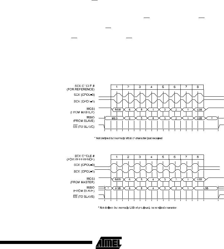
There are four combinations of SCK phase and polarity with respect to serial data, which are determined by control bits CPHA and CPOL. The SPI data transfer formats are shown in Figure 43 and Figure 44.
Figure 43. SPI Transfer Format with CPHA = 0 and DORD = 0
Figure 44. SPI Transfer Format with CPHA = 1 and DORD = 0
65
1228B–09/01