Материал: DOC1228
Note: 1. X = A or B
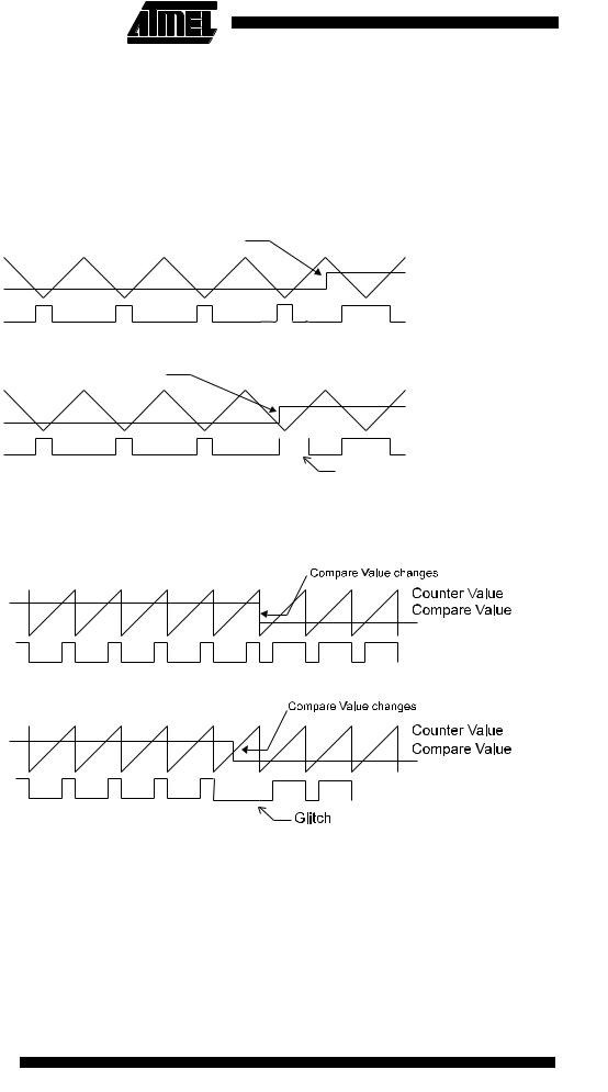
Note that in the PWM mode, the 8, 9 or 10 least significant OCR1A/OCR1B bits (depends of resolution), when written, are transferred to a temporary location. They are latched when Timer/Counter1 reaches the value TOP. This prevents the occurrence of odd-length PWM pulses (glitches) in the event of an unsynchronized OCR1A/OCR1B write. See Figure 38 and Figure 39 for an example in each mode.
Figure 38. Effects on Unsynchronized OCR1 Latching(1)
Compare Value changes
Counter Value
Compare Value
PWM Output OC1X
Synchronized OCR1X Latch
Compare Value changes
Counter Value
Compare Value
|
|
|
PWM Output OC1X |
|
|
|
|
Unsynchronized |
OCR1X Latch |
Glitch |
|
Note: 1. Note: X = A or B
Figure 39. Effects of Unsynchronized OCR1 Latching in Overflow Mode1
PWM Output OC1x
Synchronized OC1x Latch
PWM Output OC1x
Unsynchronized OC1x Latch
Note: 1. Note: X = A or B
During the time between the write and the latch operation, a read from OCR1A or OCR1B will read the contents of the temporary location. This means that the most recently written value always will read out of OCR1A/B.
When the OCR1X contains $0000 or TOP, and the up/down PWM mode is selected, the output OC1A/OC1B is updated to low or high on the next compare match according to the settings of COM1A1/COM1A0 or COM1B1/COM1B0. This is shown in Table 19. In
56 ATmega161(L)
1228B–09/01

 ATmega161(L)
overflow PWM mode, the output OC1A/OC1B is held low or high only when the Output Compare Register contains TOP.
Table 19. PWM Outputs OCR1X = $0000 or TOP(1)
COM1X1 |
COM1X0 |
OCR1X |
Output OC1X |
|
|
|
|
1 |
0 |
$0000 |
L |
|
|
|
|
1 |
0 |
TOP |
H |
|
|
|
|
1 |
1 |
$0000 |
H |
|
|
|
|
1 |
1 |
TOP |
L |
|
|
|
|
Note: 1. X = A or B
In overflow PWM mode, the table above is only valid for OCR1X = TOP.
In up/down PWM mode, the Timer Overflow Flag1 (TOV1) is set when the counter advances from $0000. In overflow PWM mode, the Timer Overflow flag is set as in normal Timer/Counter mode. Timer Overflow Interrupt1 operates exactly as in normal Timer/Counter mode, i.e., it is executed when TOV1 is set, provided that Timer Overflow Interrupt1 and global interrupts are enabled. This also applies to the Timer Output Compare1 flags and interrupts.
57
1228B–09/01
Watchdog Timer
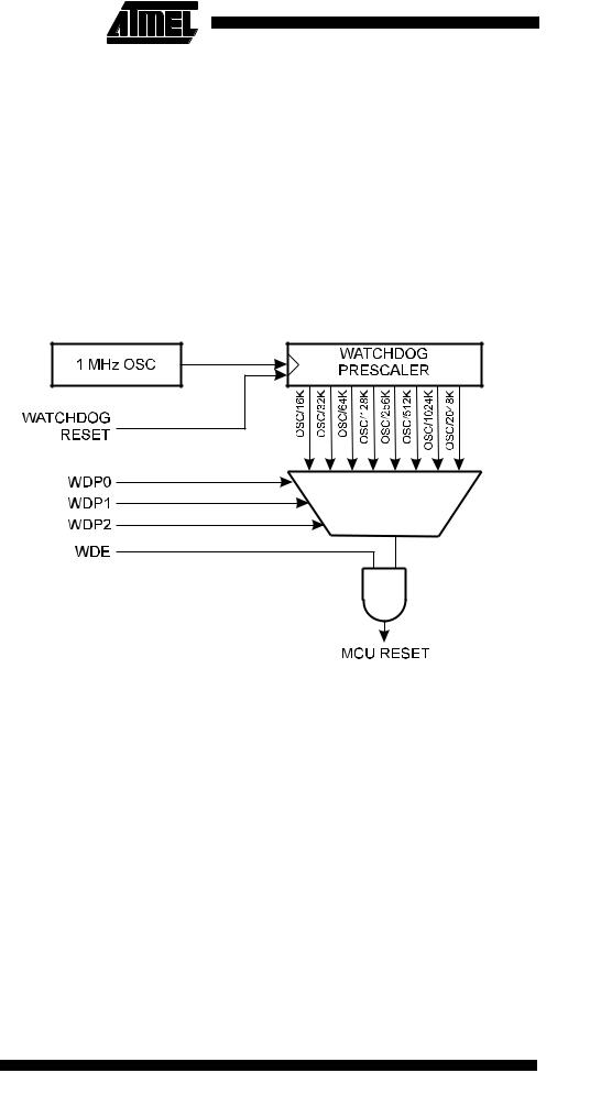
The Watchdog Timer is clocked from a separate On-chip oscillator that runs at 1 MHz. This is the typical value at VCC = 5V. See characterization data for typical values at other VCC levels. By controlling the Watchdog Timer prescaler, the Watchdog Reset interval can be adjusted (see Table 20 for a detailed description). The WDR (Watchdog Reset) instruction resets the Watchdog Timer. Eight different clock cycle periods can be selected to determine the reset period. If the reset period expires without another Watchdog reset, the ATmega161 resets and executes from the reset vector. For timing details on the Watchdog reset, refer to page 29.
To prevent unintentional disabling of the Watchdog, a special turn-off sequence must be followed when the Watchdog is disabled. Refer to the description of the Watchdog Timer Control Register for details.
Figure 40. Watchdog Timer
Watchdog Timer Control
Register – WDTCR
Bit |
7 |
6 |
5 |
4 |
3 |
2 |
1 |
0 |
|
$21 ($41) |
– |
– |
– |
WDTOE |
WDE |
WDP2 |
WDP1 |
WDP0 |
WDTCR |
|
|
|
|
|
|
|
|
|
|
Read/Write |
R |
R |
R |
R/W |
R/W |
R/W |
R/W |
R/W |
|
Initial Value |
0 |
0 |
0 |
0 |
0 |
0 |
0 |
0 |
|
• Bits 7..5 – Res: Reserved Bits
These bits are reserved bits in the ATmega161 and will always read as zero.
• Bit 4 – WDTOE: Watchdog Turn-off Enable
This bit must be set (one) when the WDE bit is cleared. Otherwise, the watchdog will not be disabled. Once set, hardware will clear this bit to zero after four clock cycles. Refer to the description of the WDE bit for a watchdog disable procedure.
• Bit 3 – WDE: Watchdog Enable
When the WDE is set (one), the Watchdog Timer is enabled and if the WDE is cleared (zero), the Watchdog Timer function is disabled. WDE can only be cleared if the WDTOE bit is set (one). To disable an enabled Watchdog Timer, the following procedure must be followed:
58 ATmega161(L)
1228B–09/01

 ATmega161(L)
1.In the same operation, write a logical “1” to WDTOE and WDE. A logical “1” must be written to WDE even though it is set to one before the disable operation starts.
2.Within the next four clock cycles, write a logical “0” to WDE. This disables the watchdog.
• Bits 2..0 – WDP2, WDP1, WDP0: Watchdog Timer Prescaler 2, 1 and 0
The WDP2, WDP1 and WDP0 bits determine the Watchdog Timer prescaling when the Watchdog Timer is enabled. The different prescaling values and their corresponding time-out periods are shown in Table 20.
Table 20. Watchdog Timer Prescale Select (1)
|
|
|
Number of WDT |
Typical Time-out |
Typical Time-out |
WDP2 |
WDP1 |
WDP0 |
Oscillator Cycles |
at VCC = 3.0V |
at VCC = 5.0V |
0 |
0 |
0 |
16K |
47 ms |
15 ms |
|
|
|
|
|
|
0 |
0 |
1 |
32K |
94 ms |
30 ms |
|
|
|
|
|
|
0 |
1 |
0 |
64K |
0.19 s |
60 ms |
|
|
|
|
|
|
0 |
1 |
1 |
128K |
0.38 s |
0.12 s |
|
|
|
|
|
|
1 |
0 |
0 |
256K |
0.75 s |
0.24 s |
|
|
|
|
|
|
1 |
0 |
1 |
512K |
1.5 s |
0.49 s |
|
|
|
|
|
|
1 |
1 |
0 |
1,024K |
3.0 s |
0.97 s |
|
|
|
|
|
|
1 |
1 |
1 |
2,048K |
6.0 s |
1.9 s |
|
|
|
|
|
|
Note: 1. The frequency of the Watchdog oscillator is voltage-dependent, as shown in the Electrical Characteristics section.
The WDR (Watchdog Reset) instruction should always be executed before the Watchdog Timer is enabled. This ensures that the reset period will be in accordance with the Watchdog Timer prescale settings. If the Watchdog Timer is enabled without reset, the Watchdog Timer may not start counting from zero.
To avoid unintentional MCU Reset, the Watchdog Timer should be disabled or reset before changing the Watchdog Timer Prescale Select.
59
1228B–09/01

EEPROM Read/Write
Access
The EEPROM access registers are accessible in the I/O space.
The write access time is in the range of 1.9 - 3.4 ms, depending on the frequency of the RC oscillator used to time the EEPROM access time. See Table 22 for details. A selftiming function, however, lets the user software detect when the next byte can be written. If the user code contains code that writes the EEPROM, some precaution must be taken. In heavily filtered power supplies, VCC is likely to rise or fall slowly on powerup/down. This causes the device for some period of time to run at a voltage lower than specified as minimum for the clock frequency used. CPU operation under these conditions is likely cause the program counter to perform unintentional jumps and eventually execute the EEPROM write code. To secure EEPROM integrity, the user is advised to use an external under-voltage reset circuit in this case.
In order to prevent unintentional EEPROM writes, a specific write procedure must be followed. Refer to the description of the EEPROM Control Register for details on this.
When the EEPROM is written, the CPU is halted for two clock cycles before the next instruction is executed. When the EEPROM is read, the CPU is halted for four clock cycles before the next instruction is executed.
EEPROM Address Register –
EEARH and EEARL
Bit |
15 |
14 |
13 |
12 |
11 |
10 |
9 |
8 |
|
$1F ($3F) |
– |
– |
– |
– |
– |
– |
– |
EEAR8 |
EEARH |
|
|
|
|
|
|
|
|
|
|
$1E ($3E) |
EEAR7 |
EEAR6 |
EEAR5 |
EEAR4 |
EEAR3 |
EEAR2 |
EEAR1 |
EEAR0 |
EEARL |
|
|
|
|
|
|
|
|
|
|
|
7 |
6 |
5 |
4 |
3 |
2 |
1 |
0 |
|
Read/Write |
R |
R |
R |
R |
R |
R |
R |
R/W |
|
|
R/W |
R/W |
R/W |
R/W |
R/W |
R/W |
R/W |
R/W |
|
Initial Value |
0 |
0 |
0 |
0 |
0 |
0 |
0 |
X |
|
|
X |
X |
X |
X |
X |
X |
X |
X |
|
• Bits 15..9 – Res: Reserved Bits
These bits are reserved bits in the ATmega161 and will always read as zero.
• Bits 8..0 – EEAR8..0: EEPROM Address
The EEPROM Address Registers (EEARH and EEARL) specify the EEPROM address in the 512-byte EEPROM space. The EEPROM data bytes are addressed linearly between 0 and 511. The initial value of EEAR is undefined. A proper value must be written before the EEPROM may be accessed.
EEPROM Data Register –
EEDR
Bit |
7 |
6 |
5 |
4 |
3 |
2 |
1 |
0 |
|
$1D ($3D) |
MSB |
|
|
|
|
|
|
LSB |
EEDR |
|
|
|
|
|
|
|
|
|
|
Read/Write |
R/W |
R/W |
R/W |
R/W |
R/W |
R/W |
R/W |
R/W |
|
Initial Value |
0 |
0 |
0 |
0 |
0 |
0 |
0 |
0 |
|
• Bits 7..0 – EEDR7..0: EEPROM Data
For the EEPROM write operation, the EEDR register contains the data to be written to the EEPROM in the address given by the EEAR register. For the EEPROM read operation, the EEDR contains the data read out from the EEPROM at the address given by EEAR.
60 ATmega161(L)
1228B–09/01