Материал: DOC1228
Asynchronous Status
Register – ASSR
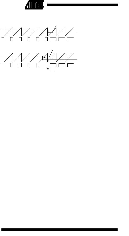
Figure 35. Effects of Unsynchronized OCR Latching in Overflow Mode.
Compare Value changes
Counter Value
Compare Value
PWM Output OCn
Synchronized OCn Latch
Compare Value changes
Counter Value
Compare Value
PWM Output OCn
Glitch
Unsynchronized OCn Latch
Note: n = 0 or 2 (Figure 34 and Figure 35)
During the time between the write and the latch operation, a read from the Output Compare Registers will read the contents of the temporary location. This means that the most recently written value always will read out of OCR0 and OCR2.
When the Output Compare Register contains $00 or $FF, and the up/down PWM mode is selected, the output PB0(OC0/PWM0)/PB1(OC2/PWM2) is updated to low or high on the next compare match according to the settings of COMn1/COMn0. This is shown in Table 13. In overflow PWM mode, the output PB0(OC0/PWM0)/PB1(OC2/PWM2) is held low or high only when the Output Compare Register contains $FF.
Table 13. PWM Outputs OCRn = $00 or $FF(1)(2)
COMn1 |
COMn0 |
OCRn |
Output PWMn |
|
|
|
|
1 |
0 |
$00 |
L |
|
|
|
|
1 |
0 |
$FF |
H |
|
|
|
|
1 |
1 |
$00 |
H |
|
|
|
|
1 |
1 |
$FF |
L |
|
|
|
|
Note: 1. n = 0 or 2
2. In overflow PWM mode, the table above is only valid for OCRn = $FF.
In up/down PWM mode, the Timer Overflow Flag (TOV0 or TOV2) is set when the counter advances from $00. In overflow PWM mode, the Timer Overflow Flag is set as in normal Timer/Counter mode. Timer Overflow Interrupt0 and 2 operate exactly as in normal Timer/Counter mode, i.e., they are executed when TOV0 or TOV2 are set, provided that Timer Overflow Interrupt and global interrupts are enabled. This also applies to the Timer Output Compare flag and interrupt.
Bit |
7 |
6 |
5 |
4 |
3 |
2 |
1 |
0 |
|
$26 ($46) |
– |
– |
– |
– |
AS2 |
TCN2UB |
OCR2UB |
TCR2UB |
ASSR |
|
|
|
|
|
|
|
|
|
|
Read/Write |
R |
R |
R |
R |
R/W |
R |
R |
R |
|
Initial Value |
0 |
0 |
0 |
0 |
0 |
0 |
0 |
0 |
|
• Bits 7..4 – Res: Reserved Bits
These bits are reserved bits in the ATmega161 and always read as zero.
46 ATmega161(L)
1228B–09/01

 ATmega161(L)
Asynchronous Operation of
Timer/Counter2
• Bit 3 – AS2: Asynchronous Timer/Counter2 Mode
When this bit is cleared (zero), Timer/Counter2 is clocked from the internal system clock, CK. If AS2 is set, the Timer/Counter2 is clocked from the TOSC1 pin. Pins PD4 and PD5 become connected to a crystal oscillator and cannot be used as general I/O pins. When the value of this bit is changed, the contents of TCNT2, OCR2 and TCCR2 might get corrupted.
• Bit 2 – TCN2UB: Timer/Counter2 Update Busy
When Timer/Counter2 operates asynchronously and TCNT2 is written, this bit becomes set (one). When TCNT2 has been updated from the temporary storage register, this bit is cleared (zero) by hardware. A logical “0” in this bit indicates that TCNT2 is ready to be updated with a new value.
• Bit 1 – OCR2UB: Output Compare Register2 Update Busy
When Timer/Counter2 operates asynchronously and OCR2 is written, this bit becomes set (one). When OCR2 has been updated from the temporary storage register, this bit is cleared (zero) by hardware. A logical “0” in this bit indicates that OCR2 is ready to be updated with a new value.
• Bit 0 – TCR2UB: Timer/Counter Control Register2 Update Busy
When Timer/Counter2 operates asynchronously and TCCR2 is written, this bit becomes set (one). When TCCR2 has been updated from the temporary storage register, this bit is cleared (zero) by hardware. A logical “0” in this bit indicates that TCCR2 is ready to be updated with a new value.
If a write is performed to any of the three Timer/Counter2 registers while its update busy flag is set (one), the updated value might get corrupted and cause an unintentional interrupt to occur.
The mechanisms for reading TCNT2, OCR2 and TCCR2 are different. When reading TCNT2, the actual timer value is read. When reading OCR2 or TCCR2, the value in the temporary storage register is read.
When Timer/Counter2 operates asynchronously, some considerations must be taken:
•Warning: When switching between asynchronous and synchronous clocking of Timer/Counter2, the timer registers TCNT2, OCR2, and TCCR2 might get corrupted. A safe procedure for switching clock source is:
1.Disable the Timer/Counter2 interrupts by clearing OCIE2 and TOIE2.
2.Select clock source by setting AS2 as appropriate.
3.Write new values to TCNT2, OCR2, and TCCR2.
4.To switch to asynchronous operation: Wait for TCN2UB, OCR2UB, and TCR2UB.
5.Enable interrupts, if needed.
•The oscillator is optimized for use with a 32,768 Hz watch crystal. An external clock signal applied to this pin goes through the same amplifier having a bandwidth of
256kHz. The external clock signal should therefore be in the interval 0 Hz -
256 kHz. The frequency of the clock signal applied to the TOSC1 pin must be lower than one fourth of the CPU main clock frequency.
•When writing to one of the registers TCNT2, OCR2, or TCCR2, the value is transferred to a temporary register, and latched after two positive edges on TOSC1. The user should not write a new value before the contents of the temporary register have been transferred to its destination. Each of the three mentioned registers have their individual temporary register, which means that e.g., writing to TCNT2 does not
47
1228B–09/01

disturb an OCR2 write in progress. To detect that a transfer to the destination register has taken place, a Asynchronous Status Register – ASSR has been implemented.
•When entering Power-save mode after having written to TCNT2, OCR2 or TCCR2, the user must wait until the written register has been updated if Timer/Counter2 is used to wake up the device. Otherwise, the MCU will go to sleep before the changes have had any effect. This is extremely important if the Output Compare2 interrupt is used to wake up the device; output compare is disabled during write to OCR2 or TCNT2. If the write cycle is not finished (i.e., the MCU enters sleep mode before the OCR2UB bit returns to zero), the device will never get a compare match and the MCU will not wake up.
•If Timer/Counter2 is used to wake up the device from Power-save mode, precautions must be taken if the user wants to re-enter Power-save mode: The interrupt logic needs one TOSC1 cycle to be reset. If the time between wake-up and re-entering Power-save mode is less than one TOSC1 cycle, the interrupt will not occur and the device will fail to wake up. If the user is in doubt whether the time before re-entering Power-save is sufficient, the following algorithm can be used to ensure that one TOSC1 cycle has elapsed:
1.Write a value to TCCR2, TCNT2, or OCR2.
2.Wait until the corresponding Update Busy flag in ASSR returns to zero.
3.Enter Power-save mode.
•When asynchronous operation is selected, the 32 kHz oscillator for Timer/Counter2 is always running, except in Power-down mode. After a Power-up Reset or wake-up from power-down, the user should be aware of the fact that this oscillator might take as long as one second to stabilize. The user is advised to wait for at least one second before using Timer/Counter2 after power-up or wake-up from power-down. The contents of all Timer/Counter2 registers must be considered lost after a wakeup from power-down, due to unstable clock signal upon start-up, regardless of whether the oscillator is in use or a clock signal is applied to the TOSC pin.
•Description of wake-up from Power-save mode when the timer is clocked asynchronously: When the interrupt condition is met, the wake-up process is started on the following cycle of the timer clock, that is, the timer is always advanced by at least 1 before the processor can read the counter value. The interrupt flags are updated three processor cycles after the processor clock has started. During these cycles, the processor executes instructions, but the interrupt condition is not readable and the interrupt routine has not started yet.
•During asynchronous operation, the synchronization of the interrupt flags for the asynchronous timer takes three processor cycles plus one timer cycle. The timer is therefore advanced by at least 1 before the processor can read the timer value, causing the setting of the interrupt flag. The output compare pin is changed on the timer clock and is not synchronized to the processor clock.
48 ATmega161(L)
1228B–09/01
ATmega161(L)
Timer/Counter1 |
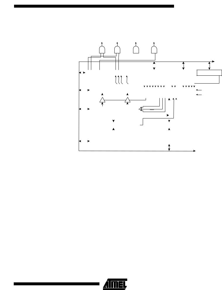
Figure 36 shows the block diagram for Timer/Counter1. |
|||
|
Figure 36. Timer/Counter1 Block Diagram |
|||
|
T/C1 OVER- |
T/C1 COMPARE |
T/C1 COMPARE |
T/C1 INPUT |
|
FLOW IRQ |
MATCHA IRQ |
MATCHB IRQ |
CAPTURE IRQ |
DATABUS |
|
|
|
OCIE1A OCIE1B |
|
|
|
|
|
|
|
|
|
|
|
|
|
|
|
|
|
|
|
|
|
|
|
|
|
|
|
|
|
|
|
|
|
|
|
|
|
|
|
|
|
|
|
|
|
|
|
|
|
|
|
|
|
|
|
|
|
|
|
OCF1A OCF1B |
|
|
|
|
|
|
|
|
|
|
|
|
|
|
|
|
|
|
|
|
|
|
|
|
|
|
|
|
|
|
|
|
|
|
|
|
|
|
|
|
|
||||||
|
|
|
|
|
|
|
|
|
|
|
|
|
|
|
|
|
|
|
|
|
|
|
|
|
|
|
|
|
|
|
|
|
|
|
|
|
|
|
|
|
|
|
|
|
|
||||||||||
TOIE1 |
TOIE2 |
TICIE1 OCIE2 |
TOIE0 |
OCIE0 |
|
|
TOV1 |
TOV2 |
ICF1 |
OCF2 |
|
TOV0 |
OCF0 |
|
|
|
|
|
|
|
|
|
|
|
|
|
|
|
|
|
|
|
|
|
|
|
|
|
|
|
|
|
|
|
|
||||||||||
|
|
|
|
|
|
|
|
|
|
|
|
|
|
|
|
|
|
|
|
|
|
|
|
|
|
|
|
|
|
|
|
|
|
|
|
||||||||||||||||||||
|
TIMER INT. MASK |
|
|
TIMER INT. FLAG |
|
|
|
|
|
T/C1 CONTROL |
|
|
|
|
|
|
T/C1 CONTROL |
|
|
||||||||||||||||||||||||||||||||||||
8-BIT |
|
REGISTER (TIMSK) |
|
|
REGISTER (TIFR) |
|
|
REGISTER A (TCCR1A) |
|
|
|
|
|
REGISTER B (TCCR1B) |
|
||||||||||||||||||||||||||||||||||||||||
|
|
|
|
|
|
|
|
|
TOV1 |
OCF1A OCF1B TOV2 |
|
ICF1 OCF2 |
|
TOV0 |
|
OCF0 |
|
|
COM1A1 |
COM1A0 |
COM1B0 |
COM1B1 |
FOC1A |
FOC1B |
PWM11 |
PWM10 |
|
|
|
|
|
|
ICNC1 |
ICES1 |
|
|
CTC1 |
CS12 |
CS11 |
CS10 |
|
|
|||||||||||||
|
|
|
|
|
|
|
|
|
|
|
|
|
|
|
|
|
|
|
|||||||||||||||||||||||||||||||||||||
|
|
|
|
|
|
|
|
|
|
|
|
|
|
|
|
|
|
|
|
|
|
|
|
|
|
|
|
|
|
|
|
|
|
|
|
|
|
|
|||||||||||||||||
|
|
|
|
15 |
|
|
|
|
|
8 |
|
7 |
|
|
|
|
|
|
|
0 |
|
|
|
|
|
|
|
|
|
|
|
|
|
|
|
|
|
|
|
|
|
|
|
|
|
|
|
|
|
||||||
|
|
|
|
|
|
|
|
|
|
|
|
|
|
|
|
|
|
|
|
|
|
|
|
|
|
|
|
|
|
|
|
|
|
|
|
|
|
|
|
|
|
|
|
|
|
|
|
|
|
|
|
|
|
|
|
|
|
|
|
|
|
T/C1 INPUT CAPTURE REGISTER (ICR1) |
|
|
|
|
|
|
|
|
|
|
|
|
CONTROL |
|
|
|
|
|
|
|
|||||||||||||||||||||||||||||
|
|
|
|
|
|
|
|
|
|
|
|
|
|
|
|
|
|
|
|
|
|
|
|
|
|||||||||||||||||||||||||||||||
|
|
|
|
|
|
|
|
|
|
|
|
|
|
|
|
|
|
|
|
|
|
|
|
|
|
|
|
|
|
|
|
|
|
|
|
|
|
LOGIC |
|
|
|
|
|
|
|
||||||||||
|
|
|
|
|
|
|
|
|
|
|
|
|
|
|
|
|
|
|
|
CAPTURE |
|
|
|
|
|
|
|
|
|
||||||||||||||||||||||||||
|
|
|
|
|
|
|
|
|
|
|
|
|
|
|
|
|
|
|
|
|
|
|
|
|
|
|
|
|
|
|
|
|
|
|
|
|
|
|
|
|
|
|
|
|
|
|
|
|
|||||||
|
|
|
|
|
|
|
|
|
|
|
|
|
|
|
|
|
|
|
|
|
|
|
|
|
|
|
|
|
|
|
|
|
|
|
|
|
|
|
|
|
|
|
|
|
|
|
|
||||||||
|
|
|
|
|
|
|
|
|
|
|
|
|
|
|
|
|
|
|
|
TRIGGER |
|
|
|
|
|
|
|
|
|
|
|
|
|
|
|
|
|
|
|
|
|
|
|
|
|
|
|
|
|
||||||
|
|
|
|
15 |
|
|
|
|
|
8 |
|
7 |
|
|
|
|
|
|
|
0 |
|
|
|
T/C CLEAR |
|
|
|
|
|
|
|
|
|
|
|
|
|
|
|
|
|
||||||||||||||
|
|
|
|
|
|
|
|
|
|
|
|
|
|
|
|
|
|
|
|
|
|
|
|
|
|
|
|
|
|
|
|
|
|
|
|
|
|||||||||||||||||||
|
|
|
|
|
|
|
|
|
|
|
|
|
|
|
|
|
|
|
|
|
|
|
|
|
|
|
|
|
|
T/C CLOCK SOURCE |
|
|
|
|
|
|
|
|
|
|
|
|
|
|
|
|
|
||||||||
|
|
|
|
|
|
|
TIMER/COUNTER1 (TCNT1) |
|
|
|
|
|
|
|
|
|
|
|
|
|
|
|
|
|
|
|
|
|
|
|
|
|
|
|
|
||||||||||||||||||||
|
|
|
|
|
|
|
|
|
|
|
|
|
|
|
|
|
|
UP/DOWN |
|
|
|
|
|
|
|
|
|
|
|
|
|
|
|
|
|
||||||||||||||||||||
|
|
|
|
|
|
|
|
|
|
|
|
|
|
|
|
|
|
|
|
|
|
|
|
|
|
|
|
|
|
|
|
|
|
|
|
|
|
|
|
|
|
|
|
|
|
|
|
|
|
|
|
|
|
|
|
|
|
|
|
|
|
|
|
|
|
|
|
|
|
|
|
|
|
|
|
|
|
|
|
|
|
|
|
|
|
|
|
|
|
|
|
|
|
|
|
|
|
|
|
|
|
|
|
|
|
||||||
|
|
|
|
|
|
|
|
|
|
|
|
|
|
|
|
|
|
|
|
|
|
|
|
|
|
|
|
|
|
|
|
|
|
|
|
|
|
|
|
|
|
|
|
|
|
|
|
|
|||||||
|
|
|
|
15 |
|
|
|
|
|
8 |
|
7 |
|
|
|
|
|
|
|
0 |
|
|
15 |
|
|
|
|
|
|
|
8 |
|
|
7 |
|
|
|
|
0 |
||||||||||||||||
|
|
|
|
|
|
|
|
|
|
|
|
|
|
|
|
|
|
|
|
|
|
||||||||||||||||||||||||||||||||||
|
|
|
|
|
|
|
|
|
|
|
|
|
|
|
|
|
|
|
|
|
|
|
|
|
|
|
|
|
|
|
|
|
|
|
|
|
|
|
|
|
|
|
|
|
|
|
|
|
|
|
|
|
|
||
|
|
|
|
|
|
|
16 BIT COMPARATOR |
|
|
|
|
|
|
|
|
|
|
|
|
|
|
|
|
16 BIT COMPARATOR |
|
|
|
|
|
|
|
||||||||||||||||||||||||
|
|
|
|
|
|
|
|
|
|
|
|
|
|
|
|
|
|
|
|
|
|
|
|
|
|
|
|||||||||||||||||||||||||||||
|
|
|
|
|
|
|
|
|
|
|
|
|
|
|
|
|
|
|
|
|
|
|
|
|
|
|
|
|
|
|
|
|
|
|
|
|
|
|
|
|
|
|
|
|
|
|
|
|
|
|
|
|
|
|
|
|
|
|
|
15 |
|
|
|
|
|
8 |
|
7 |
|
|
|
|
|
|
|
0 |
|
|
15 |
|
|
|
|
|
|
|
8 |
|
|
7 |
|
|
|
|
0 |
||||||||||||||||
|
|
|
|
|
|
|
|
|
|
|
|
|
|
|
|
|
|
|
|
|
|
|
|
|
|
|
|
|
|
|
|
||||||||||||||||||||||||
|
|
|
|
|
|
|
|
|
|
|
|
|
|
|
|
|
|
|
|
|
|
|
|
|
|
|
|
|
|
|
|
|
|
|
|
|
|
|
|
|
|
|
|
|
|
|
|
|
|
|
|
|
|||
|
|
|
|
|
TIMER/COUNTER1 OUTPUT COMPARE REGISTER A |
|
|
|
|
TIMER/COUNTER1 OUTPUT COMPARE REGISTER B |
|
||||||||||||||||||||||||||||||||||||||||||||
|
|
|
|
|
|
|
|
|
|
||||||||||||||||||||||||||||||||||||||||||||||
|
|
|
|
|
|
|
|
|
|
|
|
|
|
|
|
|
|
|
|
|
|
|
|
|
|
|
|
|
|
|
|
|
|
|
|
|
|
|
|
|
|
|
|
|
|
|
|
|
|
|
|
|
|
|
|
SPECIAL FUNCTIONS IO REGISTER (SFIOR)
PSR2 |
PSR10 |
CK
T1
The 16-bit Timer/Counter1 can select clock source from CK, prescaled CK or an external pin. In addition, it can be stopped as described in “Timer/Counter1 Control Register B – TCCR1B”. The different status flags (overflow, compare match, and capture event) are found in the Timer/Counter Interrupt Flag Register (TIFR). Control signals are found in the Timer/Counter1 Control Registers (TCCR1A and TCCR1B). The interrupt enable/disable settings for Timer/Counter1 are found in the Timer/Counter Interrupt Mask Register (TIMSK).
When Timer/Counter1 is externally clocked, the external signal is synchronized with the oscillator frequency of the CPU. To assure proper sampling of the external clock, the minimum time between two external clock transitions must be at least one internal CPU clock period. The external clock signal is sampled on the rising edge of the internal CPU clock.
The 16-bit Timer/Counter1 features both a high-resolution and a high-accuracy usage with the lower prescaling opportunities. Similarly, the high-prescaling opportunities make the Timer/Counter1 useful for lower speed functions or exact timing functions with infrequent actions.
The Timer/Counter1 supports two Output Compare functions using the Output Compare Register 1 A and B (OCR1A and OCR1B) as the data sources to be compared to the Timer/Counter1 contents. The Output Compare functions include optional clearing of the counter on compareA match and actions on the Output Compare pins on both compare matches.
49
1228B–09/01
Timer/Counter1 Control
Register A – TCCR1A
Timer/Counter1 can also be used as an 8-, 9-, or 10-bit Pulse Width Modulator. In this mode the counter and the OCR1A/OCR1B registers serve as a dual glitch-free standalone PWM with centered pulses. Alternatively, the Timer/Counter1 can be configured to operate at twice the speed in PWM mode, but without centered pulses. Refer to page 55 for a detailed description of this function.
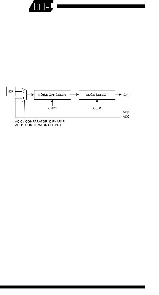
The Input Capture function of Timer/Counter1 provides a capture of the Timer/Counter1 contents to the Input Capture Register (ICR1), triggered by an external event on the Input Capture Pin (ICP). The actual capture event settings are defined by the Timer/Counter1 Control Register (TCCR1B). In addition, the Analog Comparator can be set to trigger the Input Capture. Refer to the section, “The Analog Comparator”, for details on this. The ICP pin logic is shown in Figure 37.
Figure 37. ICP Pin Schematic Diagram
If the noise canceler function is enabled, the actual trigger condition for the capture event is monitored over four samples, and all four must be equal to activate the capture flag.
Bit |
7 |
6 |
5 |
4 |
3 |
2 |
1 |
0 |
|
$2F ($4F) |
COM1A1 |
COM1A0 |
COM1B1 |
COM1B0 |
FOC1A |
FOC1B |
PWM11 |
PWM10 |
TCCR1A |
|
|
|
|
|
|
|
|
|
|
Read/Write |
R/W |
R/W |
R/W |
R/W |
R/w |
R/W |
R/W |
R/W |
|
Initial Value |
0 |
0 |
0 |
0 |
0 |
0 |
0 |
0 |
|
• Bits 7, 6 – COM1A1, COM1A0: Compare Output Mode1A, Bits 1 and 0
The COM1A1 and COM1A0 control bits determine any output pin action following a compare match in Timer/Counter1. Any output pin actions affect pin OC1A (Output CompareA pin 1). This is an alternative function to an I/O port, and the corresponding direction control bit must be set (one) to control an output pin. The control configuration is shown in Table 14.
• Bits 5, 4 – COM1B1, COM1B0: Compare Output Mode1B, Bits 1 and 0
The COM1B1 and COM1B0 control bits determine any output pin action following a compare match in Timer/Counter1. Any output pin actions affect pin OC1B (Output CompareB). This is an alternative function to an I/O port, and the corresponding direction control bit must be set (one) to control an output pin. The following control configuration is given:
50 ATmega161(L)
1228B–09/01