Материал: DOC1228
ATmega161(L)
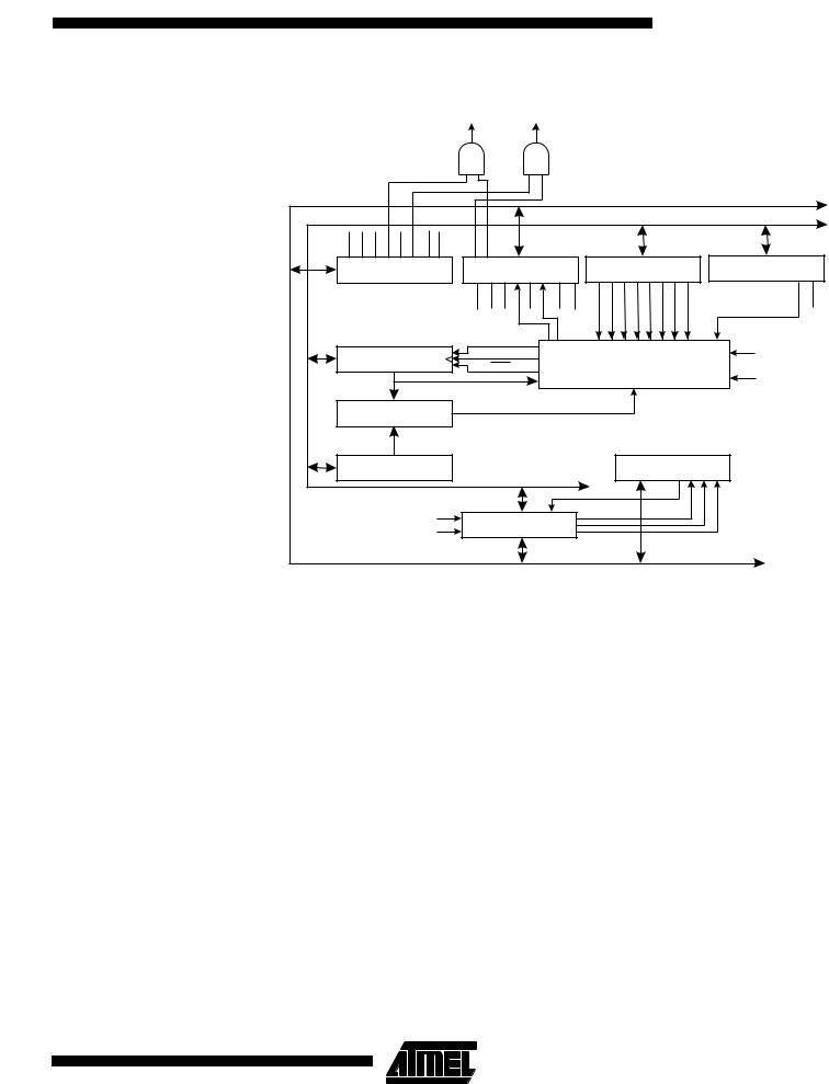
Figure 33. Timer/Counter2 Block Diagram
T/C2 OVER- T/C2 COMPARE
FLOW IRQ MATCH IRQ
8-BIT DATA BUS
|
|
|
|
|
8-BIT ASYNCH T/C2 DATA BUS |
|
|
||||
TOIE1 |
OCIE1A OCIE1B TOIE2 TICIE1 OCIE2 TOIE0 OCIE0 |
OCF2 |
TOV2 |
|
|
|
|
|
|
|
|
|
TIMER INT. MASK |
|
TIMER INT. FLAG |
|
|
|
T/C2 CONTROL |
|
SPECIAL FUNCTIONS |
||
|
REGISTER (TIMSK) |
|
REGISTER (TIFR) |
|
|
REGISTER (TCCR2) |
|
IO REGISTER (SFIOR) |
|||
|
|
TOV1 |
OCF1A OCF1B TOV2 ICF1 OCF2 |
TOV0 |
OCF0 |
FOC2 |
PWM2 |
COM21 COM20 CTC2 CS22 CS21 CS20 |
|
PSR2 |
PSR10 |
7 |
|
0 |
T/C CLEAR |
|
|
|
|
|
|
|
|
|
TIMER/COUNTER2 |
|
T/C CLK SOURCE |
|
|
|
|
CONTROL |
|
CK |
|
|
(TCNT2) |
|
UP/DOWN |
|
|
|
|
|
|
|
|
|
|
|
|
|
|
LOGIC |
|
|
|
||
|
|
|
|
|
|
|
|
|
|
||
|
|
|
|
|
|
|
|
|
TOSC1 |
|
|
|
|
|
|
|
|
|
|
|
|
|
|
7 |
|
0 |
|
|
|
|
|
|
|
|
|
|
8-BIT COMPARATOR |
|
|
|
|
|
|
|
|
|
|
7 |
|
0 |
|
|
|
|
|
|
|
|
|
|
OUTPUT COMPARE |
|
|
|
|
|
|
ASYNCH. STATUS |
|
||
|
REGISTER2 (OCR2) |
|
|
|
|
|
|
REGISTER (ASSR) |
|
||
|
CK |
|
|
|
|
|
|
AS2 TC2UB |
OCR2UB |
ICR2UB |
|
|
|
SYNCH UNIT |
|
|
|
|
|
|
|
|
|
|
TCK2 |
|
|
|
|
|
|
|
|
|
|
|
|
|
|
|
|
|
|
|
|
|
|
The 8-bit Timer/Counter0 can select clock source from CK, prescaled CK or an external pin.The 8-bit Timer/Counter2 can select clock source from CK, prescaled CK or external TOSC1.
Both Timer/Counters can be stopped as described in sections “Timer/Counter0 Control
Register – TCCR0” and “Timer/Counter2 Control Register – TCCR2”.
The various status flags (overflow and compare match) are found in the Timer/Counter
Interrupt Flag Register (TIFR). Control signals are found in the Timer/Counter Control
Register (TCCR0 and TCCR2). The interrupt enable/disable settings are found in the
Timer/Counter Interrupt Mask Register (TIMSK).
When Timer/Counter0 is externally clocked, the external signal is synchronized with the oscillator frequency of the CPU. To assure proper sampling of the external clock, the minimum time between two external clock transitions must be at least one internal CPU clock period. The external clock signal is sampled on the rising edge of the internal CPU clock.
The 8-bit Timer/Counters feature both a high resolution and a high accuracy usage with the lower prescaling opportunities. Similarly, the high prescaling opportunities make the Timer/Counter0 useful for lower speed functions or exact timing functions with infrequent actions.
Timer/Counters 0 and 2 can also be used as 8-bit Pulse Width Modulators. In this mode, the Timer/Counter and the output compare register serve as a glitch-free, standalone PWM with centered pulses. Refer to page 44 for a detailed description of this function.
41
1228B–09/01
Timer/Counter0 Control
Register – TCCR0
Timer/Counter2 Control
Register – TCCR2
|
|
|
|
|
|
|
|
|
|
|
|
|
|
|
|
|
|
|
|
|
|
|
|
|
|
|
|
|
|
|
|
|
|
|
|
|
|
|
|
|
|
|
|
|
|
|
|
|
|
|
|
|
|
|
|
|
|
|
|
|
|
|
|
|
|
|
|
Bit |
7 |
6 |
5 |
|
4 |
3 |
2 |
1 |
|
0 |
|
|||||
|
|
|
|
|
|
|
|
|
|
|
|
|
|
|||
$33 ($53) |
FOC0 |
|
PWM0 |
|
COM01 |
|
COM00 |
CTC0 |
CS02 |
CS01 |
CS00 |
TCCR0 |
||||
|
|
|
|
|
|
|
|
|
|
|
|
|
|
|
|
|
Read/Write |
R/W |
|
R/W |
|
|
|
R/W |
R/W |
R/W |
R/W |
R/W |
R/W |
|
|||
Initial Value |
0 |
0 |
0 |
|
0 |
0 |
0 |
0 |
|
0 |
|
|||||
Bit |
7 |
6 |
5 |
|
4 |
3 |
2 |
1 |
|
0 |
|
|||||
|
|
|
|
|
|
|
|
|
|
|
|
|
|
|||
$27 ($47) |
FOC2 |
|
PWM2 |
|
|
COM21 |
COM20 |
CTC2 |
CS22 |
CS21 |
|
CS20 |
TCCR2 |
|||
|
|
|
|
|
|
|
|
|
|
|
|
|
|
|
||
Read/Write |
R/W |
|
R/W |
|
|
|
R/W |
R/W |
R/W |
R/W |
R/W |
R/W |
|
|||
Initial Value |
0 |
0 |
0 |
|
0 |
0 |
0 |
0 |
|
0 |
|
|||||
• Bit 7 – FOC0/FOC2: Force Output Compare
Writing a logical “1” to this bit forces a change in the compare match output pin PB0 (Timer/Counter0) and PB1 (Timer/Counter2) according to the values already set in COMn1 and COMn0. If the COMn1 and COMn0 bits are written in the same cycle as FOC0/FOC2, the new settings will not take effect until the next compare match or Forced Output Compare match occurs. The Force Output Compare bit can be used to change the output pin without waiting for a compare match in the timer. The automatic action programmed in COMn1 and COMn0 happens as if a Compare Match had occurred, but no interrupt is generated and the Timer/Counters will not be cleared even if CTC0/CTC2 is set. The FOC0/FOC2 bits will always be read as zero. The setting of the FOC0/FOC2 bits has no effect in PWM mode.
• Bit 6 – PWM0/PWM2: Pulse Width Modulator Enable
When set (one), this bit enables PWM mode for Timer/Counter0 or Timer/Counter2. This mode is described on page 44.
• Bits 5, 4 – COM01, COM00/COM21, COM20: Compare Output Mode, Bits 1 and 0
The COMn1 and COMn0 control bits determine any output pin action following a compare match in Timer/Counter0 or Timer/Counter2. Output pin actions affect pins PB0(OC0) or PB1(OC2). This is an alternative function to an I/O port and the corresponding direction control bit must be set (one) to control an output pin. The control configuration is shown in Table 9.
Table 9. Compare Mode Select(1)(2)
COMn1 |
COMn0 |
Description |
|
|
|
0 |
0 |
Timer/Counter disconnected from output pin OCn. |
|
|
|
0 |
1 |
Toggle the OCn output line. |
|
|
|
1 |
0 |
Clear the OCn output line (to zero). |
|
|
|
1 |
1 |
Set the OCn output line (to one). |
|
|
|
Notes: 1. In PWM mode, these bits have a different function. Refer to Table 12 for a detailed description.
2.n = 0 or 2
•Bit 3 – CTC0/CTC2: Clear Timer/Counter on Compare Match
When the CTC0 or CTC2 control bit is set (one), Timer/Counter0 or Timer/Counter2 is reset to $00 in the CPU clock cycle after a compare match. If the control bit is cleared, the Timer/Counter continues counting and is unaffected by a compare match. When a prescaling of 1 is used, and the compare register is set to C, the timer will count as follows if CTC0/CTC2 is set:
... | C-1 | C | 0 | 1 | ...
42 ATmega161(L)
1228B–09/01

 ATmega161(L)
When the prescaler is set to divide by 8, the timer will count like this:
... | C-1, C-1, C-1, C-1, C-1, C-1, C-1, C-1 | C, C, C, C, C, C, C, C | 0, 0, 0, 0, 0, 0, 0, 0 |
1, 1, 1, ...
In PWM mode, this bit has a different function. If the CTC0 or CTC2 bit is cleared in PWM mode, the Timer/Counter acts as an up/down counter. If the CTC0 or CTC2 bit is set (one), the Timer/Counter wraps when it reaches $FF. Refer to page 44 for a detailed description.
• Bits 2, 1, 0 – CS02, CS01, CS00/CS22, CS21, CS20: Clock Select Bits 2, 1 and 0
The Clock Select bits 2, 1, and 0 define the prescaling source of Timer/Counter0 and
Timer/Counter2.
Table 10. Clock 0 Prescale Select
CS02 |
CS01 |
CS00 |
Description |
|
|
|
|
0 |
0 |
0 |
Stop, the Timer/Counter0 is stopped. |
|
|
|
|
0 |
0 |
1 |
CK |
|
|
|
|
0 |
1 |
0 |
CK/8 |
|
|
|
|
0 |
1 |
1 |
CK/64 |
|
|
|
|
1 |
0 |
0 |
CK/256 |
|
|
|
|
1 |
0 |
1 |
CK/1024 |
|
|
|
|
1 |
1 |
0 |
External Pin PB0(T0), falling edge |
|
|
|
|
1 |
1 |
1 |
External Pin PB0(T0), rising edge |
|
|
|
|
Table 11. Clock 2 Prescale Select
CS22 |
CS21 |
CS20 |
Description |
|
|
|
|
0 |
0 |
0 |
Stop, the Timer/Counter2 is stopped. |
|
|
|
|
0 |
0 |
1 |
PCK2 |
|
|
|
|
0 |
1 |
0 |
PCK2/8 |
|
|
|
|
0 |
1 |
1 |
PCK2/32 |
|
|
|
|
1 |
0 |
0 |
PCK2/64 |
|
|
|
|
1 |
0 |
1 |
PCK2/128 |
|
|
|
|
1 |
1 |
0 |
PCK2/256 |
|
|
|
|
1 |
1 |
1 |
PCK2/1024 |
|
|
|
|
The Stop condition provides a Timer Enable/Disable function. The prescaled modes are scaled directly from the CK oscillator clock for Timer/Counter0 and PCK2 for Timer/Counter2. If the external pin modes are used for Timer/Counter0, transitions on PB0/(T0) will clock the counter even if the pin is configured as an output. This feature can give the user software control of the counting.
43
1228B–09/01
Timer Counter0 – TCNT0
Timer/Counter2 – TCNT2
Timer/Counter0 Output
Compare Register – OCR0
Timer/Counter2 Output
Compare Register – OCR2
Timer/Counters 0 and 2 in
PWM Mode
PWM Modes (Up/Down and
Overflow)
|
|
|
|
|
|
|
|
|
|
|
|
|
|
|
|
|
|
|
|
|
|
|
|
|
|
|
|
|
|
|
|
|
|
|
|
|
|
|
|
|
|
|
|
|
|
|
|
|
|
|
|
|
|
|
|
|
|
|
|
Bit |
7 |
6 |
|
5 |
4 |
3 |
2 |
1 |
0 |
|
||||
|
|
|
|
|
|
|
|
|
|
|
|
|
|
|
$32 ($52) |
MSB |
|
|
|
|
|
|
|
|
|
|
|
LSB |
TCNT0 |
|
|
|
|
|
|
|
|
|
|
|
|
|
|
|
Read/Write |
R/W |
R/W |
|
R/W |
R/W |
R/W |
R/W |
|
R/W |
|
R/W |
|
||
Initial Value |
0 |
0 |
|
0 |
0 |
0 |
0 |
0 |
0 |
|
||||
Bit |
7 |
6 |
|
5 |
4 |
3 |
2 |
1 |
0 |
|
||||
|
|
|
|
|
|
|
|
|
|
|
|
|
|
|
$23 ($43) |
MSB |
|
|
|
|
|
|
|
|
|
|
|
LSB |
TCNT2 |
|
|
|
|
|
|
|
|
|
|
|
|
|
|
|
Read/Write |
R/W |
R/W |
|
R/W |
R/W |
R/W |
R/W |
|
R/W |
|
R/W |
|
||
Initial Value |
0 |
0 |
|
0 |
0 |
0 |
0 |
0 |
0 |
|
||||
These 8-bit registers contain the value of the Timer/Counters.
Both Timer/Counters are realized as up or up/down (in PWM mode) counters with read and write access. If the Timer/Counter is written to and a clock source is selected, it continues counting in the timer clock cycle following the write operation.
Bit |
7 |
6 |
5 |
4 |
3 |
2 |
1 |
0 |
|
$31 ($51) |
MSB |
|
|
|
|
|
|
LSB |
OCR0 |
|
|
|
|
|
|
|
|
|
|
Read/Write |
R/W |
R/W |
R/W |
R/W |
R/W |
R/W |
R/W |
R/W |
|
Initial Value |
0 |
0 |
0 |
0 |
0 |
0 |
0 |
0 |
|
Bit |
7 |
6 |
5 |
4 |
3 |
2 |
1 |
0 |
|
|
|
|
|
|
|
|
|
|
|
$22 ($42) |
MSB |
|
|
|
|
|
|
LSB |
OCR2 |
|
|
|
|
|
|
|
|
|
|
Read/Write |
R/W |
R/W |
R/W |
R/W |
R/W |
R/W |
R/W |
R/W |
|
Initial Value |
0 |
0 |
0 |
0 |
0 |
0 |
0 |
0 |
|
The output compare registers are 8-bit read/write registers. The Timer/Counter Output Compare Registers contain the data to be continuously compared with the Timer/Counter. Actions on compare matches are specified in TCCR0 and TCCR2. A software write to the Timer/Counter Register blocks compare matches in the next Timer/Counter clock cycle. This prevents immediate interrupts when initializing the Timer/Counter.
A compare match will set the compare interrupt flag in the CPU clock cycle following the compare event.
When PWM mode is selected, the Timer/Counter either wraps (overflows) when it reaches $FF or it acts as an up/down counter.
If the up/down mode is selected, the Timer/Counter and the Output Compare Registers (OCR0 or OCR2) form an 8-bit, free-running, glitch-free and phase-correct PWM with outputs on the PB0(OC0/PWM0) or PB1(OC2/PWM2) pin.
If the overflow mode is selected, the Timer/Counter and the Output Compare Registers (OCR0 or OCR2) form an 8-bit, free-running and glitch-free PWM, operating with twice the speed of the up/down counting mode.
The two different PWM modes are selected by the CTC0 or CTC2 bit in the Timer/Counter Control Registers – TCCR0 or TCCR2, respectively.
If CTC0/CTC2 is cleared and PWM mode is selected, the Timer/Counter acts as an up/down counter, counting up from $00 to $FF, where it turns and counts down again to zero before the cycle is repeated. When the counter value matches the contents of the Output Compare Register, the PB0(OC0/PWM0) or PB1(OC2/PWM2) pin is set or
44 ATmega161(L)
1228B–09/01
 ATmega161(L)
cleared according to the settings of the COMn1/COMn0 bits in the Timer/Counter Control Registers TCCR0 or TCCR2.
If CTC0/CTC2 is set and PWM mode is selected, the Timer/Counters will wrap and start counting from $00 after reaching $FF. The PB0(OC0/PWM0) or PB1(OC2/PWM2) pin will be set or cleared according to the settings of COMn1/COMn0 on a Timer/Counter overflow or when the counter value matches the contents of the Output Compare Register. Refer to Table 12 for details.
Table 12. Compare Mode Select in PWM Mode(1)
CTCn |
COMn1 |
COMn0 |
Effect on Compare Pin |
Frequency |
|
|
|
|
|
|
|
0 |
0 |
0 |
Not connected |
|
|
|
|
|
|
|
|
0 |
0 |
1 |
Not connected |
|
|
|
|
|
|
|
|
|
|
|
Cleared on compare match, up-counting. Set on |
fTCK0/2/510 |
|
0 |
1 |
0 |
compare match, down-counting (non-inverted |
||
|
|
|
PWM). |
|
|
|
|
|
|
|
|
0 |
1 |
1 |
Cleared on compare match, down-counting. Set |
fTCK0/2/510 |
|
on compare match, up-counting (inverted PWM). |
|||||
|
|
|
|
||
|
|
|
|
|
|
1 |
0 |
0 |
Not connected |
|
|
|
|
|
|
|
|
1 |
0 |
1 |
Not connected |
|
|
|
|
|
|
|
|
1 |
1 |
0 |
Cleared on compare match, set on overflow |
fTCK0/2/256 |
|
1 |
1 |
1 |
Set on compare match, cleared on overflow |
fTCK0/2/256 |
|
Note: |
1. n = 0 or 2 |
|
|
||
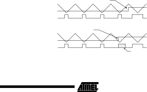
Note that in PWM mode, the value to be written to the Output Compare Register is first transferred to a temporary location and then latched into the OCR when the Timer/Counter reaches $FF. This prevents the occurrence of odd-length PWM pulses (glitches) in the event of an unsynchronized OCR0 or OCR2 write. See Figure 34 and Figure 35 for examples.
Figure 34. Effects of Unsynchronized OCR Latching in Up/Down Mode
Compare Value changes
Counter Value
Compare Value
PWM Output OCn
Synchronized OCn Latch
Compare Value changes
Counter Value
Compare Value
PWM Output OCn
Unsynchronized OCn Latch Glitch
45
1228B–09/01