Материал: DOC1228
Features
•High-performance, Low-power AVR® 8-bit Microcontroller
•Advanced RISC Architecture
–130 Powerful Instructions – Most Single Clock Cycle Execution
–32 x 8 General Purpose Working Registers
–Fully Static Operation
–Up to 8 MIPS Throughput at 8 MHz
–On-chip 2-cycle Multiplier
•Program and Data Memories
–16K Bytes of Nonvolatile In-System Programmable Flash Endurance: 1,000 Write/Erase Cycles
–Optional Boot Code Memory with Independent Lock Bits Self-programming of Program and Data Memories
–512 Bytes of Nonvolatile In-System Programmable EEPROM Endurance: 100,000 Write/Erase Cycles
–1K Byte of Internal SRAM
–Programming Lock for Software Security
•Peripheral Features
–Two 8-bit Timer/Counters with Separate Prescaler and PWM
–Expanded 16-bit Timer/Counter System with Separate Prescaler, Compare, Capture Modes and Dual 8-, 9-, or 10-bit PWM
–Dual Programmable Serial UARTs
–Master/Slave SPI Serial Interface
–Real-time Counter with Separate Oscillator
–Programmable Watchdog Timer with Separate On-chip Oscillator
–On-chip Analog Comparator
•Special Microcontroller Features
–Power-on Reset and Programmable Brown-out Detection
–External and Internal Interrupt Sources
–Three Sleep Modes: Idle, Power-save and Power-down
•Power Comsumption at 4 MHz, 3.0V, 25°C
–Active 3.0 mA
–Idle Mode 1.2 mA
–Power-down Mode < 1 µA
•I/O and Packages
–35 Programmable I/O Lines
–40-lead PDIP and 44-lead TQFP
•Operating Voltages
–2.7V - 5.5V for the ATmega161L
–4.0V - 5.5V for the ATmega161
•Speed Grades
–0 - 4 MHz for the ATmega161L
–0 - 8 MHz for the ATmega161
•Commercial and Industrial Temperature Ranges
8-bit  Microcontroller with 16K Bytes of In-System Programmable Flash
ATmega161
ATmega161L
Rev. 1228B–09/01
1
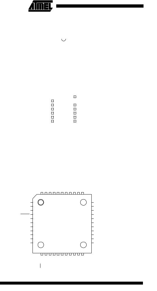
Pin Configuration
PDIP
(OC0/T0) PB0 |
|
1 |
40 |
|
VCC |
||||||
|
|
||||||||||
(OC2/T1) PB1 |
|
2 |
39 |
|
PA0 (AD0) |
||||||
|
|
||||||||||
(RXD1/AIN0) PB2 |
|
3 |
38 |
|
PA1 (AD1) |
||||||
|
|
||||||||||
(TXD1/AIN1) PB3 |
|
4 |
37 |
|
PA2 (AD2) |
||||||
|
|
||||||||||
|
|
|
|
|
|
|
|
|
|
||
(SS) PB4 |
|
5 |
36 |
|
PA3 (AD3) |
||||||
|
|
||||||||||
(MOSI) PB5 |
|
6 |
35 |
|
PA4 (AD4) |
||||||
|
|
||||||||||
(MISO) PB6 |
|
7 |
34 |
|
PA5 (AD5) |
||||||
|
|
||||||||||
(SCK) PB7 |
|
8 |
33 |
|
PA6 (AD6) |
||||||
|
|
||||||||||
|
|
|
|
|
|
|
|
9 |
32 |
|
|
|
|
RESET |
|
|
PA7 (AD7) |
||||||
|
|
||||||||||
(RXD0) PD0 |
|
10 |
31 |
|
PE0 (ICP/INT2) |
||||||
|
|
||||||||||
(TXD0) PD1 |
|
11 |
30 |
|
PE1 (ALE) |
||||||
|
|
||||||||||
(INT0) PD2 |
|
12 |
29 |
|
PE2 (OC1B) |
||||||
|
|
||||||||||
(INT1) PD3 |
|
13 |
28 |
|
PC7 (A15) |
||||||
|
|
||||||||||
(TOSC1) PD4 |
|
14 |
27 |
|
PC6 (A14) |
||||||
|
|
||||||||||
(OC1A/TOSC2) PD5 |
|
15 |
26 |
|
PC5 (A13) |
||||||
|
|||||||||||
|
|
|
|
16 |
25 |
|
PC4 (A12) |
||||
|
(WR) |
PD6 |
|
|
|||||||
|
|
PD7 |
|
17 |
24 |
|
PC3 (A11) |
||||
(RD) |
|
|
|||||||||
|
|
|
XTAL2 |
|
18 |
23 |
|
PC2 (A10) |
|||
|
|
|
XTAL1 |
|
19 |
22 |
|
PC1 (A9) |
|||
|
|
|
|
|
GND |
|
20 |
21 |
|
PC0 (A8) |
|
|
|
|
|
|
|
|
|
|
|
|
|
TQFP
PB4 (SS) |
PB3 (TXD1/AIN1) |
PB2 (RXD1/AIN0) |
PB1 (OC2/T1) |
PB0 (OC0/T0) |
NC* |
VCC |
PA0 (AD0) |
PA1 (AD1) |
PA2 (AD2) |
PA3 (AD3) |
44 |
43 |
42 |
41 |
40 |
39 |
38 |
37 |
36 |
35 |
34 |
(MOSI) PB5 
 1 (MISO) PB6
  2 (SCK) PB7
 3
3
RESET  4 (RXD0) PD0
 5 NC*
5 NC*  6 (TXD0) PD1
 7 (INT0) PD2
  8 (INT1) PD3
 9
9
(TOSC1) PD4  10 (OCIA/TOSC2) PD5
 11
11
12 |
13 |
14 |
15 |
16 |
17 |
18 |
19 |
20 |
21 |
22 |
|
(WR) PD6 |
|
(RD) PD7 |
XTAL2 |
XTAL1 |
GND |
NC* |
(A8) PC0 |
(A9) PC1 |
(A10) PC2 |
(A11) PC3 |
(A12) PC4 |
|
|
|
|||||||||
|
|
|
|
|
|||||||
33  PA4 (AD4)
32 
 PA5 (AD5)
31 
 PA6 (AD6)
30  PA7 (AD7)
29 
 PE0 (ICP/INT2)
28  NC*
NC*
27 
 PE1 (ALE)
26  PE2 (OC1B)
25 
 PC7 (A15)
24  PC6 (A14)
23 
 PC5 (A13)
* NC = Do not connect
(Can be used in future devices)
2 ATmega161(L)
1228B–09/01

 ATmega161(L)
Description
The ATmega161 is a low-power CMOS 8-bit microcontroller based on the AVR RISC architecture. By executing powerful instructions in a single clock cycle, the ATmega161 achieves throughputs approaching 1 MIPS per MHz allowing the system designer to optimize power consumption versus processing speed. The AVR core combines a rich instruction set with 32 general purpose working registers. All the 32 registers are directly connected to the Arithmetic Logic Unit (ALU), allowing two independent registers to be accessed in one single instruction executed in one clock cycle. The resulting architecture is more code-efficient while achieving throughputs up to ten times faster than conventional CISC microcontrollers.
The ATmega161 provides the following features: 16K bytes of In-System or Selfprogrammable Flash, 512 bytes EEPROM, 1K byte of SRAM, 35 general-purpose I/O lines, 32 general purpose working registers, Real-time Counter, 3 flexible timer/counters with compare modes, internal and external interrupts, 2 programmable serial UARTs, programmable Watchdog Timer with internal oscillator, an SPI serial port and 3 soft- ware-selectable power saving modes. The Idle mode stops the CPU while allowing the SRAM, timer/counters, SPI port and interrupt system to continue functioning. The Power-down mode saves the register and SRAM contents but freezes the oscillator, disabling all other chip functions until the next external interrupt or hardware reset. In Power-save mode, the timer oscillator continues to run, allowing the user to maintain a timer base while the rest of the device is sleeping.
The device is manufactured using Atmel’s high-density nonvolatile memory technology. The On-chip Flash program memory can be reprogrammed using the self-programming capability through the boot block and an ISP through the SPI port, or by using a conventional nonvolatile memory programmer. By combining an enhanced RISC 8-bit CPU with In-System Programmable Flash on a monolithic chip, the Atmel ATmega161 is a powerful microcontroller that provides a highly flexible and cost-effective solution to many embedded control applications.
The ATmega161 AVR is supported with a full suite of program and system development tools including: C compilers, macro assemblers, program debugger/simulators, in-circuit emulators and evaluation kits.
3
1228B–09/01
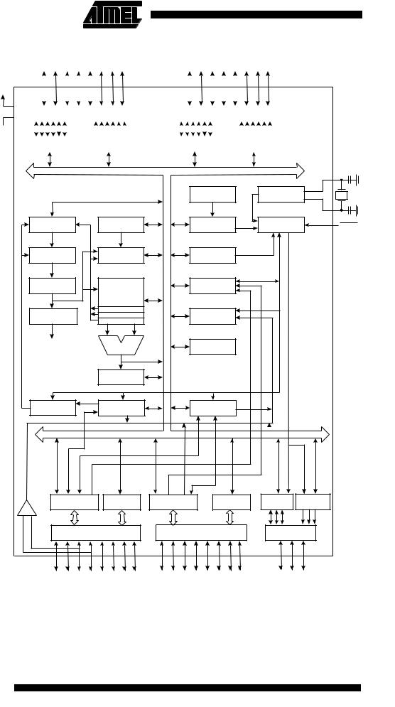
Block Diagram
Figure 1. The ATmega161 Block Diagram
|
|
|
|
|
|
|
|
|
|
|
|
|
|
PA0-PA7 |
|
|
|
|
|
|
|
|
|
|
|
|
|
|
|
|
PC0-PC7 |
|
|
|
|
|
|
|
||||||||
|
|
|
|
|
|
|
|
|
|
|
|
|
|
|
|
|
|
|
|
|
|
|
|
|
|
|
|
|
|
|
|
|||||||||||||||
VCC |
|
|
|
|
|
|
|
|
|
|
|
|
|
|
|
|
|
|
|
|
|
|
|
|
|
|
|
|
|
|
|
|
|
|
|
|
|
|
||||||||
|
|
|
|
|
|
|
|
|
|
|
|
|
|
|
|
|
|
|
|
|
|
|
|
|
|
|
|
|
|
|
|
|
|
|
||||||||||||
|
|
|
|
|
|
|
|
|
|
|
|
|
|
|
|
|
|
|
|
|
|
|
|
|
|
|
|
|
|
|
|
|
|
|
|
|
|
|
|
|
|
|
|
|
|
|
|
|
|
|
|
|
|
|
|
|
|
PORTA DRIVERS |
|
|
|
|
|
|
PORTC DRIVERS |
||||||||||||||||||||||||||||
|
|
|
|
|
|
|
|
|
|
|
|
|
|
|
|
|
|
|
|
|
|
|
|
|
|
|
|
|
|
|
|
|
|
|
|
|
|
|
|
|
|
|
|
|
|
|
|
|
|
|
|
|
|
|
|
|
|
|
|
|
|
|
|
|
|
|
|
|
|
|
|
|
|
|
|
|
|
|
|
|
|
|
|
|
|
|
|
|
|
|
|
|
|
GND |
|
|
|
|
|
|
|
|
|
|
|
|
|
|
|
|
|
|
|
|
|
|
|
|
|
|
|
|
|
|
|
|
|
|
|
|
|
|
|
|
|
|||||
|
|
|
|
|
|
|
|
|
|
|
|
|
|
|
|
|
|
|
|
|
|
|
|
|
|
|
|
|
|
|
|
|
|
|
|
|
|
|
|
|
||||||
|
|
|
|
|
|
DATA REGISTER |
|
|
|
|
|
DATA DIR. |
|
DATA REGISTER |
|
|
|
|
|
DATA DIR. |
||||||||||||||||||||||||||
|
|
|
|
|
|
|
PORTA |
|
|
|
|
REG. PORTA |
|
|
PORTC |
|
|
|
|
REG. PORTC |
||||||||||||||||||||||||||
|
|
|
8-BIT DATA BUS |
|
|
|
|
|
|
|
|
|
|
|
XTAL1 |
|
|
|
|
INTERNAL |
OSCILLATOR |
|
|
|
|
|
|
OSCILLATOR |
|
||
|
|
|
|
|
|
|
|
|
PROGRAM |
STACK |
|
WATCHDOG |
TIMING AND |
XTAL2 |
|
|
|
RESET |
|||||
|
COUNTER |
POINTER |
|
TIMER |
CONTROL |
|
|
|
|
|
|
||||
PROGRAM |
SRAM |
MCU CONTROL |
|
|
|
||
|
FLASH |
|
REGISTER |
|
|
|
|
|
|
|
|
|
|
||
INSTRUCTION |
GENERAL |
|
TIMER/ |
|
|
|
|
|
REGISTER |
PURPOSE |
|
COUNTERS |
|
|
|
|
|
REGISTERS |
|
|
|
|
|
INSTRUCTION |
X |
|
INTERRUPT |
|
|
|
|
Y |
|
|
|
|
|||
|
DECODER |
Z |
|
UNIT |
|
|
|
|
CONTROL |
ALU |
|
EEPROM |
|
|
|
|
LINES |
|
|
|
|
||
|
|
|
|
|
|
|
|
|
|
STATUS |
|
|
|
|
|
|
|
REGISTER |
|
|
|
|
|
PROGRAMMING |
SPI |
|
UARTS |
|
|
|
|
|
LOGIC |
|
|
|
|
||
|
|
|
|
|
|
|
|
ANALOG COMPARATOR |
|
|
|
|
DATA REG. |
REG. PORTE |
|
|
DATA REGISTER |
DATA DIR. |
DATA REGISTER |
DATA DIR. |
PORTE |
|
|
|
PORTB |
REG. PORTB |
PORTD |
REG. PORTD |
|
|
|
- + |
PORTB DRIVERS |
PORTD DRIVERS |
PORTE DRIVERS |
PB0 - PB7 |
PD0 - PD7 |
PE0 - PE2 |
|
|
4 ATmega161(L)
1228B–09/01

|
|
|
|
|
ATmega161(L) |
|
|
|
|
|
|
|
|
|
|
|
|
|
|
|
|
|
|
|
Pin Descriptions |
|
|
||
|
VCC |
Supply voltage. |
|||
|
GND |
Ground. |
|||
|
Port A (PA7..PA0) |
Port A is an 8-bit bi-directional I/O port. Port pins can provide internal pull-up resistors |
|||
|
|
|
|
(selected for each bit). The Port A output buffers can sink 20 mA and can drive LED dis- |
|
|
|
|
|
plays directly. When pins PA0 to PA7 are used as inputs and are externally pulled low, |
|
|
|
|
|
they will source current if the internal pull-up resistors are activated. The Port A pins are |
|
|
|
|
|
tri-stated when a reset condition becomes active, even if the clock is not running. |
|
|
|
|
|
Port A serves as a Multiplexed Address/Data port when using external memory |
|
|
|
|
|
interface. |
|
|
Port B (PB7..PB0) |
Port B is an 8-bit bi-directional I/O port with internal pull-up resistors. The Port B output |
|||
|
|
|
|
buffers can sink 20 mA. As inputs, Port B pins that are externally pulled low will source |
|
|
|
|
|
current if the pull-up resistors are activated. The Port B pins are tri-stated when a reset |
|
|
|
|
|
condition becomes active, even if the clock is not running. |
|
|
|
|
|
Port B also serves the functions of various special features of the ATmega161 as listed |
|
|
|
|
|
on page 90. |
|
|
Port C (PC7..PC0) |
Port C is an 8-bit bi-directional I/O port with internal pull-up resistors. The Port C output |
|||
|
|
|
|
buffers can sink 20 mA. As inputs, Port C pins that are externally pulled low will source |
|
|
|
|
|
current if the pull-up resistors are activated. The Port C pins are tri-stated when a reset |
|
|
|
|
|
condition becomes active, even if the clock is not running. |
|
|
|
|
|
Port C also serves as an address high output when using external memory interface. |
|
|
Port D (PD7..PD0) |
Port D is an 8-bit bi-directional I/O port with internal pull-up resistors. The Port D output |
|||
|
|
|
|
buffers can sink 20 mA. As inputs, Port D pins that are externally pulled low will source |
|
|
|
|
|
current if the pull-up resistors are activated. The Port D pins are tri-stated when a reset |
|
|
|
|
|
condition becomes active, even if the clock is not running. |
|
|
|
|
|
Port D also serves the functions of various special features of the ATmega161 as listed |
|
|
|
|
|
on page 99. |
|
|
Port E (PE2..PE0) |
Port E is a 3-bit bi-directional I/O port with internal pull-up resistors. The Port E output |
|||
|
|
|
|
buffers can sink 20 mA. As inputs, Port E pins that are externally pulled low will source |
|
|
|
|
|
current if the pull-up resistors are activated. The Port E pins are tri-stated when a reset |
|
|
|
|
|
condition becomes active, even if the clock is not running. |
|
|
|
|
|
Port E also serves the functions of various special features of the ATmega161 as listed |
|
|
|
|
|
on page 105. |
|
|
|
|
|
Reset input. A low level on this pin for more than 500 ns will generate a reset, even if the |
|
|
RESET |
||||
|
|
|
|
clock is not running. Shorter pulses are not guaranteed to generate a reset. |
|
|
XTAL1 |
Input to the inverting oscillator amplifier and input to the internal clock operating circuit. |
|||
|
XTAL2 |
Output from the inverting oscillator amplifier. |
|||
5
1228B–09/01