Материал: DOC1228

Table 8. Interrupt 0 Sense Control
ISC01 |
ISC00 |
Description |
|
|
|
0 |
0 |
The low level of INT0 generates an interrupt request. |
|
|
|
0 |
1 |
Any logical change on INT0 generates an interrupt request. |
|
|
|
1 |
0 |
The falling edge of INT0 generates an interrupt request. |
|
|
|
1 |
1 |
The rising edge of INT0 generates an interrupt request. |
|
|
|
Extended MCU Control |
The Extended MCU Control Register contains control bits for external interrupt 2, sleep |
|||||||||
Register – EMCUCR |
mode bit and control bits for the external memory interface. |
|
|
|
||||||
|
Bit |
7 |
6 |
5 |
4 |
3 |
2 |
1 |
0 |
|
|
|
|
|
|
|
|
|
|
|
|
|
$36 ($56) |
SM0 |
SRL2 |
SRL1 |
SRL0 |
SRW01 |
SRW00 |
SRW11 |
ISC2 |
EMCUCR |
|
|
|
|
|
|
|
|
|
|
|
|
Read/Write |
R/W |
R/W |
R/W |
R/W |
R/W |
R/W |
R/W |
R/W |
|
|
Initial Value |
0 |
0 |
0 |
0 |
0 |
0 |
0 |
0 |
|
• Bit 7 – SM0: Sleep Mode Bit 0
When this bit is set (one) and sleep mode bit 1 (SM1) in MCUCR is set, Power-save mode is selected as sleep mode. Refer to page 37 for a detailed description of the sleep modes.
• Bits 6..4 – SRL2, SRL1, SRL0: External SRAM Limit
It is possible to configure different wait states for different external memory addresses in ATmega161. The SRL2 - SRL0 bits are used to define at which address the different wait states will be configured. See “Interface to External Memory” on page 82 for a detailed description.
• Bits 3..1 – SRW01, SRW00, SRW11: External SRAM Wait State Select Bits
The SRW01, SRW00 and SRW11 bits are used to set up extra wait states in the external memory interface. See “Interface to External Memory” on page 82 for a detailed description.
• Bit 0 – ISC2: Interrupt Sense Control 2
The external interrupt 2 is activated by the external pin INT2 if the SREG I-flag and the corresponding interrupt mask in the GIMSK are set. If ISC2 is cleared (zero), a falling edge on INT2 activates the interrupt. If ISC2 is set (one), a rising edge on INT2 activates the interrupt. Edges on INT2 are registered asynchronously. Pulses on INT2 wider than 50 ns will generate an interrupt. Shorter pulses are not guaranteed to generate an interrupt.
When changing the ISC2 bit, an interrupt can occur. Therefore, it is recommended to first disable INT2 by clearing its Interrupt Enable bit in the GIMSK register. Then, ISC2 bit can be changed. Finally, the INT2 interrupt flag should be cleared by writing a logical “1” to its Interrupt Flag bit in the GIFR register before the interrupt is re-enabled.
36 ATmega161(L)
1228B–09/01

 ATmega161(L)
Sleep Modes
To enter any of the three sleep modes, the SE bit in MCUCR must be set (one) and a SLEEP instruction must be executed. The SM1 bit in the MCUCR register and SM0 bit in the EMCUCR register select which sleep mode (Idle, Power-down or Power-save) will be activated by the SLEEP instruction (see Table 6). If an enabled interrupt occurs while the MCU is in a sleep mode, the MCU awakes. The CPU is then halted for four cycles, it executes the interrupt routine, and resumes execution from the instruction following SLEEP. The contents of the register file, SRAM and I/O memory are unaltered. If a reset occurs during sleep mode, the MCU wakes up and executes from the Reset vector.
Idle Mode |
When the SM1/SM0 bits are set to 00, the SLEEP instruction makes the MCU enter the |
|
Idle mode, stopping the CPU but allowing SPI, UARTs, Analog Comparator, |
|
Timer/Counters, Watchdog, and the Interrupt System to continue operating. This |
|
enables the MCU to wake up from external triggered interrupts as well as internal ones |
|
like the Timer Overflow and UART Receive Complete interrupts. If wake-up from the |
|
Analog Comparator interrupt is not required, the Analog Comparator can be powered |
|
down by setting the ACD bit in the Analog Comparator Control and Status register |
|
(ACSR). This will reduce power consumption in Idle mode. |
Power-down Mode |
When the SM1/SM0 bits are set to 10, the SLEEP instruction makes the MCU enter the |
|
Power-down mode. In this mode, the external oscillator is stopped while the external |
|
interrupts and the Watchdog (if enabled) continue operating. Only an external reset, a |
|
Watchdog reset (if enabled), an external level interrupt on INT0 or INT1, or an external |
|
edge interrupt on INT2 can wake up the MCU. |
|
If INT2 is used for wake-up from Power-down mode, the edge is remembered until the |
|
MCU wakes up. |
|
If a level-triggered interrupt is used for wake-up from Power-down mode, the changed |
|
level must be held for some time to wake up the MCU. This makes the MCU less sensi- |
|
tive to noise. The changed level is sampled twice by the Watchdog oscillator clock, and |
|
if the input has the required level during this time, the MCU will wake up. The period of |
|
the Watchdog oscillator is 1 µs (nominal) at 5.0V and 25°C. The frequency of the Watch- |
|
dog oscillator is voltage-dependent as shown in the Electrical Characteristics section. |
|
When waking up from Power-down mode, a delay from the wake-up condition occurs |
|
until the wake-up becomes effective. This allows the clock to restart and become stable |
|
after having been stopped. The wake-up period is defined by the same CKSEL fuses |
|
that define the reset time-out period. The wake-up period is equal to the clock counting |
|
part of the reset period, as shown in Table 4. If the wake-up condition disappears before |
|
the MCU wakes up and starts to execute, e.g., a low level on INT0 is not held long |
|
enough, the interrupt causing the wake-up will not be executed. |
Power-save Mode |
When the SM1/SM0 bits are 11, the SLEEP instruction makes the MCU enter the |
|
Power-save mode. This mode is identical to Power-down, with one exception. |
|
If Timer/Counter2 is clocked asynchronously, i.e., the AS2 bit in ASSR is set, |
|
Timer/Counter2 will run during sleep. In addition to the Power-down wake-up sources, |
|
the device can also wake up from either Timer Overflow or Output Compare event from |
|
Timer/Counter2 if the corresponding Timer/Counter2 interrupt enable bits are set in |
|
TIMSK and the global interrupt enable bit in SREG is set. |
|
If the asynchronous timer is not clocked asynchronously, Power-down mode is recom- |
|
mended instead of Power-save mode because the contents of the register in the |
|
asynchronous timer should be considered undefined after wake-up in Power-save mode |
|
even if AS2 is 0. |
37
1228B–09/01
Timer/Counters
Timer/Counter
Prescalers
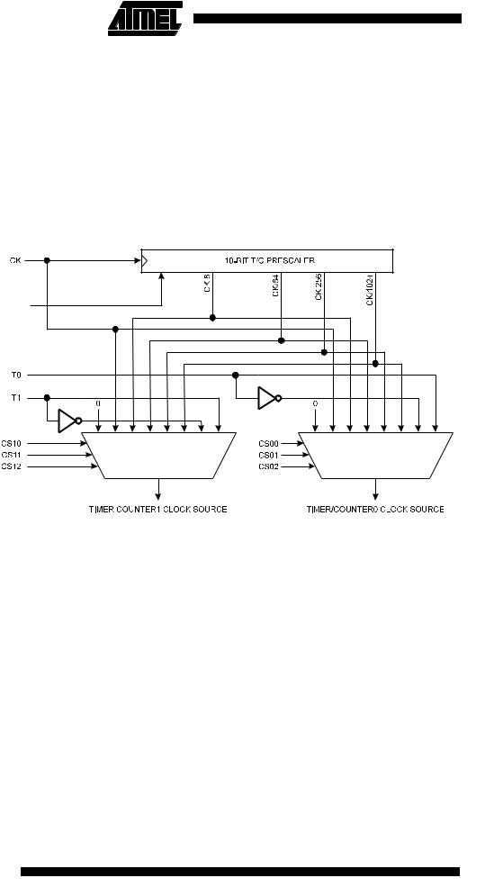
The ATmega161 provides three general purpose Timer/Counters – two 8-bit T/Cs and one 16-bit T/C. Timer/Counter2 can optionally be asynchronously clocked from an external oscillator. This oscillator is optimized for use with a 32.768 kHz watch crystal, enabling use of Timer/Counter2 as a Real-time Clock (RTC). Timer/Counters 0 and 1 have individual prescaling selection from the same 10-bit prescaling timer. Timer/Counter2 has its own prescaler. Both these prescalers can be reset by setting the corresponding control bits in the Special Functions IO Register (SFIOR). Refer to page 39 for a detailed description. These Timer/Counters can either be used as a timer with an internal clock time base or as a counter with an external pin connection, which triggers the counting.
Figure 30. Prescaler for Timer/Counter0 and 1
Clear |
PSR10 |
TCK1 |
TCK0 |
For Timer/Counters 0 and 1, the four prescaled selections are: CK/8, CK/64, CK/256, and CK/1024, where CK is the oscillator clock. For the two Timer/Counters 0 and 1, CK, external source and stop can also be selected as clock sources. Setting the PSR10 bit in SFIOR resets the prescaler. This allows the user to operate with a predictable prescaler. Note that Timer/Counter1 and Timer/Counter0 share the same prescaler and a prescaler reset will affect both Timer/Counters.
38 ATmega161(L)
1228B–09/01
 ATmega161(L)
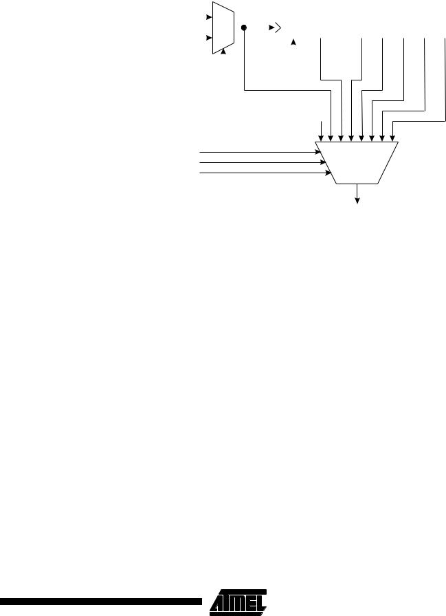
Figure 31. Timer/Counter2 Prescaler
CK |
|
|
|
PCK2 |
|
|
|
|
|
|
|
||
|
|
|
|
|
10-BIT T/C PRESCALER |
|
|
||||||
|
|
|
|
|
|
|
|
|
|||||
TOSC1 |
|
|
|
|
|
Clear |
|
|
|||||
|
|
|
|
|
|
|
|||||||
|
|
|
|
|
|
|
|
|
|
||||
|
|
|
|
|
|
PCK2/8 |
PCK2/32 |
PCK2/64 |
PCK2/128 |
PCK2/256 |
PCK2/1024 |
||
AS2 |
|
|
|
|
|
|
|||||||
|
|
|
|
|
|
||||||||
|
|
|
|
|
|||||||||
|
|
|
|
|
|
|
|
|
|
|
|
||
PSR2 |
|
|
|
|
|
|
|
|
0 |
|
|
|
|
|
|
|
|
|
|
|
|
|
|
|
|
||
|
|
|
|
|
|
|
|
|
|
|
|
|
|
CS20
CS21
CS22
Special Function IO Register –
SFIOR
TIMER/COUNTER2 CLOCK SOURCE
TCK2
The clock source for Timer/Counter2 prescaler is named PCK2. PCK2 is by default connected to the main system clock (CK). By setting the AS2 bit in ASSR, Timer/Counter2 is asynchronously clocked from the PD4(TOSC1) pin. This enables use of Timer/Counter2 as a Real-time Clock (RTC). When AS2 is set, pins PD4(TOSC1) and PD5(TOSC2) are disconnected from Port D. A crystal can then be connected between the PD4(TOSC1) and PD5(TOSC2) pins to serve as an independent clock source for Timer/Counter2. The oscillator is optimized for use with a 32.768 kHz crystal. Alternatively, an external clock signal can be applied to PD4(TOSC1). The frequency of this clock must be lower than one fourth of the CPU clock and not higher than 256 kHz. Setting the PSR2 bit in SFIOR resets the prescaler. This allows the user to operate with a predictable prescaler.
Bit |
7 |
6 |
5 |
4 |
3 |
2 |
1 |
0 |
|
$30 ($50) |
– |
– |
– |
– |
– |
– |
PSR2 |
PSR10 |
SFIOR |
|
|
|
|
|
|
|
|
|
|
Read/Write |
R |
R |
R |
R |
R |
R |
R/W |
R/W |
|
Initial Value |
0 |
0 |
0 |
0 |
0 |
0 |
0 |
0 |
|
• Bits 7..2 – Res: Reserved Bits
These bits are reserved bits in the ATmega161 and always read as zero.
• Bit 1 – PSR2: Prescaler Reset Timer/Counter2
When this bit is set (one), the Timer/Counter2 prescaler will be reset. The bit will be cleared by hardware after the operation is performed. Writing a zero to this bit will have no effect. This bit will always be read as zero if Timer/Counter2 is clocked by the internal CPU clock. If this bit is written when Timer/Counter2 is operating in asynchronous mode, however, the bit will remain as one until the prescaler has been reset. See “Asynchronous Operation of Timer/Counter2” on page 47 for a detailed description of asynchronous operation.
39
1228B–09/01
8-bit Timer/Counters
T/C0 and T/C2
• Bit 0 – PSR10: Prescaler Reset Timer/Counter1 and Timer/Counter0
When this bit is set (one), the Timer/Counter1 and Timer/Counter0 prescaler will be reset. The bit will be cleared by hardware after the operation is performed. Writing a zero to this bit will have no effect. Note that Timer/Counter1 and Timer/Counter0 share the same prescaler and a reset of this prescaler will affect both timers. This bit will always be read as zero.
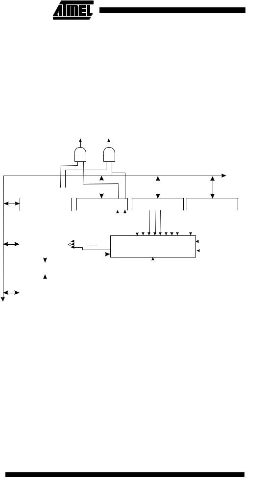
Figure 32 shows the block diagram for Timer/Counter0. Figure 33 shows the block diagram for Timer/Counter2.
Figure 32. Timer/Counter0 Block Diagram
T/C0 OVER- T/C0 COMPARE
FLOW IRQ MATCH IRQ
8-BIT DATA BUS
TOIE1 |
|
OCIE1A |
|
OCIE1B |
|
TOIE2 |
|
TICIE1 |
|
OCIE2 |
|
TOIE0 |
|
OCIE0 |
|
|
TOV0 |
OCF0 |
|
|
|
|
|
|
|
|
|
||||||||||
|
||||||||||||||||||
|
|
|
|
|
|
|
|
|
|
|
|
|
|
|
|
|
|
|
TIMER INT. MASK |
|
|
|
|
|
TIMER INT. FLAG |
|
|
|
|
|
T/C0 CONTROL |
|
|
|
|
SPECIAL FUNCTIONS |
||||||||||||||||||
REGISTER (TIMSK) |
|
|
|
|
|
REGISTER (TIFR) |
|
|
|
|
REGISTER (TCCR0) |
|
|
IO REGISTER (SFIOR) |
|||||||||||||||||||||
|
|
|
|
|
TOV1 |
|
OCF1A |
|
OCF1B |
TOV2 |
ICF1 |
OCF2 |
TOV0 |
|
OCF0 |
|
|
FOC0 |
PWM0 |
COM01 COM00 CTC0 CS02 |
CS01 |
|
CS00 |
|
|
|
|
|
|
|
PSR2 |
PSR10 |
|
||
7 |
|
0 |
|
|
|
|
|
|
|
|
|
|
|
|
|
|
|
|
|
|
|
|
|
|
|
|
|
|
|
|
|
|
|
||
|
|
|
|
|
T/C CLEAR |
|
|
|
|
|
|
|
|
|
|
|
|
|
|
|
|
|
|
|
|
|
|
||||||||
|
|
|
|
|
|
|
|
|
|
|
|
|
|
|
|
|
|
|
|
|
|
|
|
|
|
|
|||||||||
|
|
|
|
|
|
|
|
|
|
|
|
|
|
|
|
|
|
|
|
|
|
|
|
|
|
|
|||||||||
TIMER/COUNTER0 |
|
|
|
|
|
T/C CLK SOURCE |
|
|
|
|
|
|
|
CONTROL |
|
|
|
|
|
|
|
|
CK |
||||||||||||
|
|
|
|
|
|
|
|
|
|
|
|
|
|
|
|
|
|
|
|||||||||||||||||
(TCNT0) |
|
|
|
|
|
UP/DOWN |
|
|
|
|
|
|
|
|
|
|
|
|
|
|
|
|
|
|
|||||||||||
|
|
|
|
|
|
|
|
|
|
|
|
LOGIC |
|
|
|
|
|
|
|
|
|
|
|
||||||||||||
|
|
|
|
|
|
|
|
|
|
|
|
|
|
|
|
|
|
|
|
|
|
T0 |
|||||||||||||
|
|
|
|
|
|
|
|
|
|
|
|
|
|
|
|
|
|
|
|
|
|
|
|
|
|
|
|
|
|
|
|
|
|||
7 |
|
0 |
|
|
|
|
|
|
|
|
|
|
|
|
|
|
|
|
|
|
|
|
|
|
|
|
|
|
|
|
|
|
|
|
|
|
|
|
|
|
|
|
|
|
|
|
|
|
|
|
|
|
|
|
|
|
|
|
|
|
|
|
|
|
|
|
|
|
|
||
8-BIT COMPARATOR |
|
|
|
|
|
|
|
|
|
|
|
|
|
|
|
|
|
|
|
|
|
|
|
|
|
|
|
|
|
|
|
|
|
|
|
|
|
|
|
|
|
|
|
|
|
|
|
|
|
|
|
|
|
|
|
|
|
|
|
|
|
|
|
|
|
|
|
|
|
||
|
|
|
|
|
|
|
|
|
|
|
|
|
|
|
|
|
|
|
|
|
|
|
|
|
|
|
|
|
|
|
|
|
|
|
|
7 |
|
0 |
|
|
|
|
|
|
|
|
|
|
|
|
|
|
|
|
|
|
|
|
|
|
|
|
|
|
|
|
|
|
|
|
|
|
|
|
|
|
|
|
|
|
|
|
|
|
|
|
|
|
|
|
|
|
|
|
|
|
|
|
|
|
|
|
|
|
|
||
OUTPUT COMPARE |
|
|
|
|
|
|
|
|
|
|
|
|
|
|
|
|
|
|
|
|
|
|
|
|
|
|
|
|
|
|
|
|
|
|
|
REGISTER0 (OCR0) |
|
|
|
|
|
|
|
|
|
|
|
|
|
|
|
|
|
|
|
|
|
|
|
|
|
|
|
|
|
|
|
|
|
|
|
|
|
|
|
|
|
|
|
|
|
|
|
|
|
|
|
|
|
|
|
|
|
|
|
|
|
|
|
|
|
|
|
|
|
|
|
40 ATmega161(L)
1228B–09/01