Материал: DOC1228

|
|
|
|
|
|
|
|
|
|
|
|
|
|
|
|
|
|
|
|
|
|
|
|
|
|
|
|
|
|
|
|
|
|
|
|
|
|
|
|
|
|
|
|
|
|
|
|
|
|
|
|
|
|
|
|
|
|
|
|
|
|
|
|
|
|
|
|
|
|
|
|
Table 3. Reset Characteristics (V = 5.0V)(1) |
|
|
|
|
|
|
|
||||||||||
|
|
|
|
|
|
|
CC |
|
|
|
|
|
|
|
|
|
|
Symbol |
Parameter |
|
Condition |
|
Min |
Typ |
|
Max |
|
Units |
|||||||
|
|
|
|
|
|
|
|
|
|
|
|
|
|||||
|
|
Power-on Reset Threshold |
|
BOD disabled |
|
1.0 |
1.4 |
|
1.8 |
|
V |
||||||
|
|
Voltage (rising) |
|
|
|
|
|
|
|
|
|
|
|||||
VPOT |
|
BOD enabled |
|
1.7 |
2.2 |
|
2.7 |
|
V |
||||||||
|
|
|
|
|
|
|
|
|
|
||||||||
|
|
|
|
|
|
|
|
|
|
|
|
|
|
|
|
||
Power-on Reset Threshold |
|
BOD disabled |
|
0.4 |
0.6 |
|
0.8 |
|
V |
||||||||
|
|
|
|
|
|
||||||||||||
|
|
Voltage (falling)(1) |
|
|
|
|
|
|
|
|
|
|
|||||
|
|
|
BOD enabled |
|
1.7 |
2.2 |
|
2.7 |
|
V |
|||||||
|
|
|
|
|
|
|
|
|
|
|
|
||||||
|
|
|
|
|
|
|
|
|
|
|
|
|
|
|
|||
|
|
|
|
Pin Threshold |
|
|
|
|
|
|
|
|
|
|
|||
VRST |
RESET |
|
|
|
|
|
|
0.85 VCC |
|
V |
|||||||
Voltage |
|
|
|
|
|
|
|
|
|||||||||
VBOT |
Brown-out Reset Threshold |
|
(BODLEVEL = 1) |
|
2.6 |
2.7 |
|
2.8 |
|
V |
|||||||
Voltage |
|
|
|
|
|
|
|
|
|
|
|||||||
|
(BODLEVEL = 0) |
|
3.8 |
4.0 |
|
4.2 |
|
|
|||||||||
|
|
|
|
|
|
|
|
|
|
|
|
|
|||||
|
|
|
|
|
|
|
|
|
|
||||||||
Note: 1. |
The Power-on Reset will not work unless the supply voltage has been below VPOT |
||||||||||||||||
|
|
(falling). |
|
|
|
|
|
|
|
|
|
||||||
‘ |
|
|
|
|
|
|
|
|
|
|
|
|
|
|
|
|
|
Table 4. Reset Delay Selections(4) |
|
|
|
|
|
|
|
|
|
||||||||
CKSEL |
|
Start-up Time, VCC = 2.7V, |
Start-up Time, VCC = 4.0V, |
|
Recommended |
||||||||||||
[2:0] |
|
BODLEVEL Unprogrammed |
BODLEVEL Programmed |
|
Usage(1) |
|
|||||||||||
000 |
|
4.2 ms + 6 CK |
5.8 ms + 6 CK |
|
|
|
External Clock, Fast |
||||||||||
|
|
|
|
|
|
|
|
|
|
|
|
|
|
Rising Power |
|
||
|
|
|
|
|
|
|
|
||||||||||
001 |
|
30 µs + 6 CK |
10 µs + 6 CK |
|
|
|
External Clock, |
||||||||||
|
|
|
|
|
|
|
|
|
|
|
|
|
|
BOD Enabled(2)(3) |
|||
010 |
|
67 ms + 16K CK |
92 ms + 16K CK |
|
|
|
Crystal Oscillator, |
||||||||||
|
|
|
|
|
|
|
|
|
|
|
|
|
|
Slowly Rising |
|
||
|
|
|
|
|
|
|
|
|
|
|
|
|
|
Power |
|
||
|
|
|
|
|
|
|
|
||||||||||
011 |
|
4.2 ms + 16K CK |
5.8 ms + 16K CK |
|
|
|
Crystal Oscillator, |
||||||||||
|
|
|
|
|
|
|
|
|
|
|
|
|
|
Fast Rising Power |
|||
|
|
|
|
|
|
|
|
||||||||||
100 |
|
30 µs + 16K CK |
10 µs + 16K CK |
|
|
|
Crystal Oscillator, |
||||||||||
|
|
|
|
|
|
|
|
|
|
|
|
|
|
BOD Enabled(2)(3) |
|||
101 |
|
67 ms + 1K CK |
92 ms + 1K CK |
|
|
|
Ceramic |
|
|||||||||
|
|
|
|
|
|
|
|
|
|
|
|
|
|
Resonator/External |
|||
|
|
|
|
|
|
|
|
|
|
|
|
|
|
Clock, Slowly Rising |
|||
|
|
|
|
|
|
|
|
|
|
|
|
|
|
Power |
|
||
|
|
|
|
|
|
|
|
||||||||||
110 |
|
4.2 ms + 1K CK |
5.8 ms + 1K CK |
|
|
|
Ceramic Resonator, |
||||||||||
|
|
|
|
|
|
|
|
|
|
|
|
|
|
Fast Rising Power |
|||
|
|
|
|
|
|
|
|
||||||||||
111 |
|
30 µs + 1K CK |
10 µs + 1K CK |
|
|
|
Ceramic Resonator, |
||||||||||
|
|
|
|
|
|
|
|
|
|
|
|
|
|
BOD Enabled(2)(3) |
|||
Notes: 1. The CKSEL fuses control only the start-up time. The oscillator is the same for all selections. On Power-up, the real-time part of the start-up time is increased with typ.
0.6 ms.
2.Or external Power-on Reset.
3.When BOD is enabled, there will be a real-time part = 50 µs (typ)
4.Table 4 shows the start-up times from reset. From sleep, only the clock counting part of the start-up time is used. The watchdog oscillator is used for timing the real-time part of the start-up time. The number WDT oscillator cycles used for each time-out is shown in Table 5.
26 ATmega161(L)
1228B–09/01
 ATmega161(L)
Table 5. Number of Watchdog Oscillator Cycles(1)
BODLEVEL |
Time-out |
Number of Cycles |
|
|
|
Unprogrammed |
4.2 ms (at VCC = 2.7V) |
1K |
|
|
|
Unprogrammed |
67 ms (at VCC = 2.7V) |
16K |
|
|
|
Programmed |
5.8 ms (at VCC = 4.0V) |
4K |
|
|
|
Programmed |
92 ms (at VCC = 4.0V) |
64K |
|
|
|
|
Note: 1. The BOD-LEVEL fuse can be used to select start-up times even if the brown-out |
|||||||||||||
|
|
|
detection is disabled (by leaving the BODEN fuse unprogrammed). |
|||||||||||
|
The frequency of the watchdog oscillator is voltage-dependent as shown in the Electri- |
|||||||||||||
|
cal Characteristics section. The device is shipped with CKSEL = 010. |
|||||||||||||
Power-on Reset |
A Power-on Reset (POR) pulse is generated by an On-chip detection circuit. The detec- |
|||||||||||||
|
tion level is nominally 1.4V (rising VCC). The POR is activated whenever VCC is below |
|||||||||||||
|
the detection level. The POR circuit can be used to trigger the start-up reset, as well as |
|||||||||||||
|
detect a failure in supply voltage. |
|||||||||||||
|
A Power-on Reset (POR) circuit ensures that the device is reset from Power-on. Reach- |
|||||||||||||
|
ing the Power-on Reset threshold voltage invokes a delay counter, which determines |
|||||||||||||
|
the delay, for which the device is kept in RESET after VCC rise. The time-out period of |
|||||||||||||
|
the delay counter can be defined by the user through the CKSEL fuses. The eight differ- |
|||||||||||||
|
ent selections for the delay period are presented in Table 4. The RESET signal is |
|||||||||||||
|
activated again, without any delay, when the VCC decreases below detection level. |
|||||||||||||
|
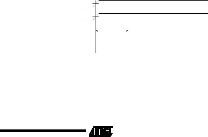
Figure 25. MCU Start-up, |
|
|
|
Tied to VCC |
|||||||||
|
RESET |
|||||||||||||
|
|
VCC |
|
|
|
|
VPOT |
|||||||
|
|
|
|
|
|
|
|
|
|
|
|
|
|
|
|
|
|
|
|
|
|
VRST |
|||||||
|
|
RESET |
|
|
|
|||||||||
|
|
|
|
|
|
|
|
|
|
|
|
|
|
|
|
TIME-OUT |
|
|
|
|
|
|
tTOUT |
|
|
|
|
||
|
|
|
|
|
|
|
|
|
|
|||||
|
|
|
|
|
|
|
|
|
|
|||||
|
INTERNAL |
|
|
|
|
|
|
|
|
|
|
|
|
|
|
|
|
|
|
|
|
|
|
|
|
|
|
||
|
RESET |
|
|
|
|
|
|
|
|
|
|
|
|
|
27
1228B–09/01
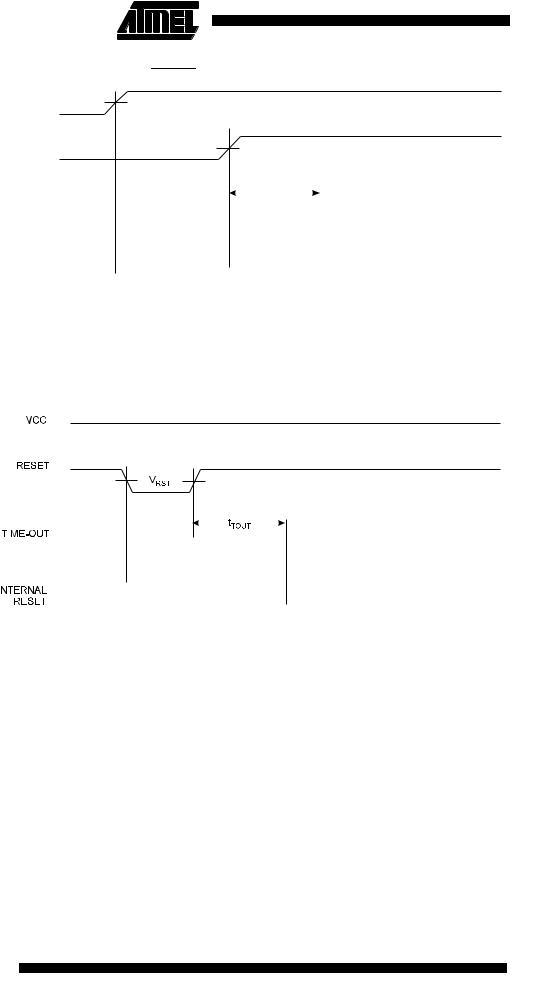
Figure 26. MCU Start-up, RESET Controlled Externally
|
|
|
|
|
|
|
|
|
VPOT |
|||||||||||||
|
|
|
|
VCC |
||||||||||||||||||
|
|
|
|
|
|
|
|
|
|
|
|
VRST |
||||||||||
|
|
|
|
|
|
|
|
|||||||||||||||
|
|
|
|
RESET |
||||||||||||||||||
|
|
|
|
|
|
|
|
|
|
|
|
|
|
tTOUT |
|
|
|
|
||||
|
|
|
|
|
|
|
|
|
|
|
|
|
|
|
|
|
|
|||||
|
|
|
|
|
|
|
|
|
|
|
|
|
||||||||||
|
|
TIME-OUT |
|
|
|
|||||||||||||||||
|
|
|
|
|
|
|
|
|
|
|
|
|
|
|
|
|
|
|||||
|
INTERNAL |
|
|
|
|
|
|
|
|
|
|
|
|
|
|
|
||||||
External Reset |
|
|
RESET |
|
|
|
|
|
|
|
|
|
|
|
|
|
|
|
||||
An External Reset is generated by a low level on the |
|
|
|
pin. Reset pulses longer |
||||||||||||||||||
RESET |
||||||||||||||||||||||
|
than 500 ns will generate a reset, even if the clock is not running. Shorter pulses are not |
|||||||||||||||||||||
|
guaranteed to generate a reset. When the applied signal reaches the Reset Threshold |
|||||||||||||||||||||
|
Voltage (VRST) on its positive edge, the delay timer starts the MCU after the Time-out |
|||||||||||||||||||||
|
period (tTOUT) has expired. |
|||||||||||||||||||||
|
Figure 27. External Reset during Operation |
|||||||||||||||||||||
|
|
|
|
|
|
|
|
|
|
|
|
|
|
|
|
|
|
|
|
|
|
|
|
|
|
|
|
|
|
|
|
|
|
|
|
|
|
|
|
|
|
|
|
|
|
|
|
|
|
|
|
|
|
|
|
|
|
|
|
|
|
|
|
|
|
|
|
|
|
|
|
|
|
|
|
|
|
|
|
|
|
|
|
|
|
|
|
|
|
|
|
|
|
|
|
|
|
|
|
|
|
|
|
|
|
|
|
|
|
|
|
|
|
|
|
|
|
|
|
|
|
|
|
|
|
|
|
|
|
|
|
|
|
|
|
|
|
|
|
|
|
|
|
|
|
|
|
|
|
|
|
|
|
|
|
|
|
|
|
|
|
|
|
|
|
|
|
|
|
|
|
|
|
|
|
|
|
|
|
|
|
|
|
Brown-out Detection |
ATmega161 has an On-chip Brown-out Detection (BOD) circuit for monitoring the VCC |
|
level during the operation. The BOD circuit can be enabled/disabled by the fuse |
|
BODEN. When BODEN is enabled (BODEN programmed), and VCC decreases to a |
|
value below the trigger level, the Brown-out Reset is immediately activated. When VCC |
|
increases above the trigger level, the Brown-out Reset is deactivated after a delay. The |
|
delay is defined by the user in the same way as the delay of POR signal in Table 4. The |
|
trigger level for the BOD can be selected by the fuse BODLEVEL to be 2.7V |
|
(BODLEVEL unprogrammed), or 4.0V (BODLEVEL programmed). The trigger level has |
|
a hysteresis of 50 mV to ensure spike-free brown-out detection. |
|
The BOD circuit will only detect a drop in VCC if the voltage stays below the trigger level |
|
for longer than 9 µs for trigger level 4.0V, 21 µs for trigger level 2.7V (typical values). |
28 ATmega161(L)
1228B–09/01
|
|
|
ATmega161(L) |
|||
|
|
|
||||
|
|
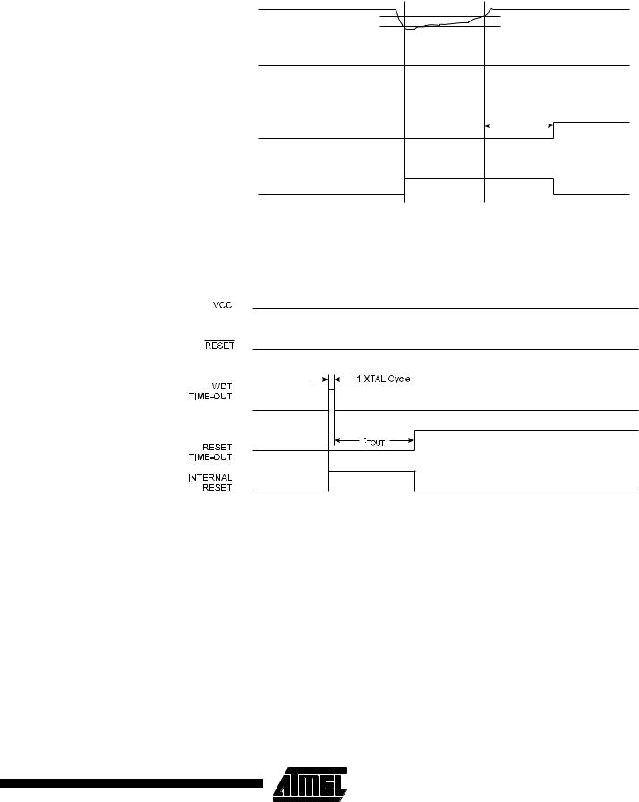
Figure 28. Brown-out Reset during Operation |
||||
|
|
|
|
|
|
|
|
|
|
|
|
|
|
|
|
VCC |
|
VBOT+ |
||
|
|
VBOT- |
|
|
|
|
|
|
RESET |
|
|
|
|
|
|
TIME-OUT |
|
tTOUT |
|
|
|
|
|
|
|||
|
|
INTERNAL |
|
|
|
|
|
|
RESET |
|
|
|
|
Watchdog Reset |
When the Watchdog times out, it will generate a short reset pulse of 1 XTAL cycle dura- |
|||||
|
|
tion. On the falling edge of this pulse, the delay timer starts counting the Time-out period |
||||
|
|
(tTOUT). Refer to page 58 for details on operation of the Watchdog. |
||||
Figure 29. Watchdog Reset during Operation
MCU Status Register – |
The MCU Status Register provides information on which reset source caused an MCU |
|||||||||
MCUSR |
reset. |
|
|
|
|
|
|
|
|
|
|
Bit |
7 |
6 |
5 |
4 |
3 |
2 |
1 |
0 |
|
|
|
|
|
|
|
|
|
|
|
|
|
$34 ($54) |
– |
– |
– |
– |
WDRF |
BORF |
EXTRF |
PORF |
MCUSR |
|
|
|
|
|
|
|
|
|
|
|
|
Read/Write |
R |
R |
R |
R |
R/W |
R/W |
R/W |
R/W |
|
|
Initial Value |
0 |
0 |
0 |
0 |
|
See Bit Description |
|||
• Bits 7..4 – Res: Reserved Bits
These bits are reserved bits in the ATmega161 and always read as zero.
• Bit 3 – WDRF: Watchdog Reset Flag
This bit is set if a Watchdog reset occurs. The bit is cleared by a Power-on Reset or by writing a logical “0” to the flag.
29
1228B–09/01

|
|
|
|
|
|
|
|
|
|
|
|
|
|
|
|
|
|
|
|
|
|
|
|
|
• Bit 2 – BORF: Brown-out Reset Flag |
||||
|
This bit is set if a Brown-out Reset occurs. The bit is cleared by a Power-on Reset or by |
||||
|
writing a logical “0” to the flag. |
||||
|
• Bit 1 – EXTRF: External Reset Flag |
||||
|
This bit is set if an External Reset occurs. The bit is cleared by a Power-on Reset or by |
||||
|
writing a logical “0” to the flag. |
||||
|
• Bit 0 – PORF: Power-on Reset Flag |
||||
|
This bit is set if a Power-on Reset occurs. The bit is cleared only by writing a logical “0” |
||||
|
to the flag. |
||||
|
To make use of the reset flags to identify a reset condition, the user should read and |
||||
|
then clear the MCUSR as early as possible in the program. If the register is cleared |
||||
|
before another reset occurs, the source of the reset can be found by examining the reset |
||||
|
flags. |
||||
Interrupt Handling |
The ATmega161 has two 8-bit Interrupt Mask control registers; GIMSK (General Inter- |
||||
|
rupt Mask register) and TIMSK (Timer/Counter Interrupt Mask register). |
||||
|
When an interrupt occurs, the Global Interrupt Enable I-bit is cleared (zero) and all inter- |
||||
|
rupts are disabled. The user software can set (one) the I-bit to enable nested interrupts. |
||||
|
The I-bit is set (one) when a Return from Interrupt instruction (RETI) is executed. |
||||
|
When the Program Counter is vectored to the actual interrupt vector in order to execute |
||||
|
the interrupt handling routine, hardware clears the corresponding flag that generated the |
||||
|
interrupt. Some of the interrupt flags can also be cleared by writing a logical “1” to the |
||||
|
flag bit position(s) to be cleared. |
||||
|
If an interrupt condition occurs when the corresponding interrupt enable bit is cleared |
||||
|
(zero), the interrupt flag will be set and remembered until the interrupt is enabled or the |
||||
|
flag is cleared by software. |
||||
|
If one or more interrupt conditions occur when the global interrupt enable bit is cleared |
||||
|
(zero), the corresponding interrupt flag(s) will be set and remembered until the global |
||||
|
interrupt enable bit is set (one), and will be executed by order of priority. |
||||
|
Note that external level interrupt does not have a flag and will only be remembered for |
||||
|
as long as the interrupt condition is present. |
||||
|
Note that the status register is not automatically stored when entering an interrupt rou- |
||||
|
tine or restored when returning from an interrupt routine. This must be handled by |
||||
|
software. |
||||
Interrupt Response Time |
The interrupt execution response for all the enabled AVR interrupts is four clock cycles |
||||
|
minimum. After four clock cycles, the program vector address for the actual interrupt |
||||
|
handling routine is executed. During this four-clock-cycle period, the Program Counter |
||||
|
(13 bits) is pushed onto the Stack. The vector is normally a jump to the interrupt routine, |
||||
|
and this jump takes three clock cycles. If an interrupt occurs during execution of a multi- |
||||
|
cycle instruction, this instruction is completed before the interrupt is served. If an inter- |
||||
|
rupt occurs when the MCU is in sleep mode, the interrupt execution response time is |
||||
|
increased by four clock cycles. |
||||
|
A return from an interrupt handling routine takes four clock cycles. During these four |
||||
|
clock cycles, the Program Counter (2 bytes) is popped back from the Stack, the Stack |
||||
|
Pointer is incremented by 2, and the I-flag in SREG is set. When AVR exits from an |
||||
|
interrupt, it will always return to the main program and execute one more instruction |
||||
|
before any pending interrupt is served. |
||||
30 ATmega161(L)
1228B–09/01