Материал: DOC1228
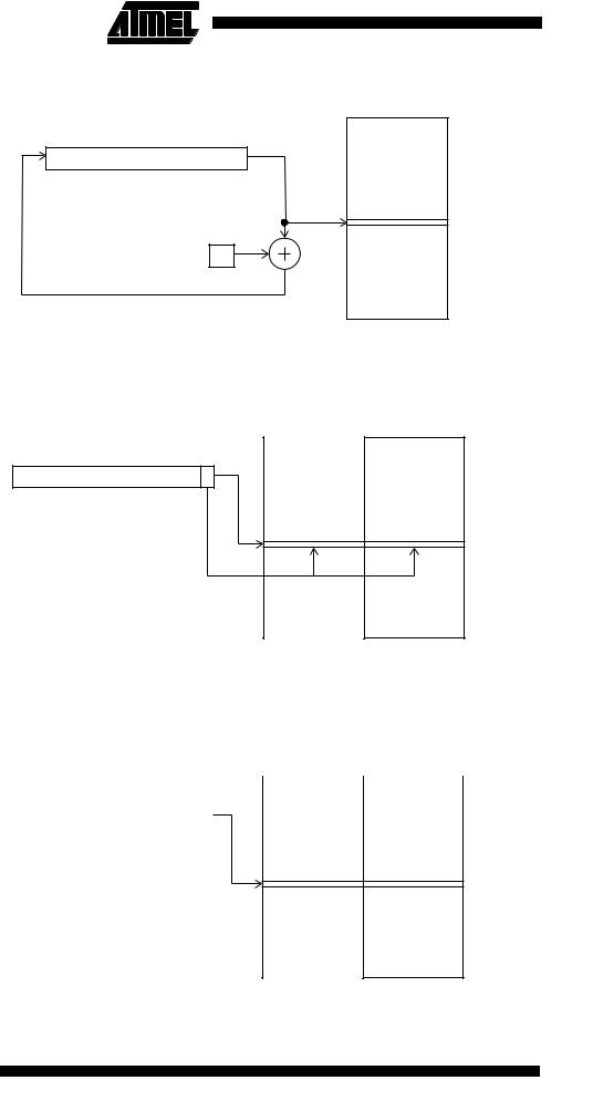
Data Indirect with Postincrement
Constant Addressing Using
the LPM Instruction
Figure 16. Data Indirect Addressing with Post-increment
Data Space
$0000
15 |
0 |
X, Y, OR Z - REGISTER
1
$FFFF
The X-, Y-, or Z-register is incremented after the operation. Operand address is the contents of the X-, Y-, or Z-register prior to incrementing.
Figure 17. Code Memory Constant Addressing
PROGRAM MEMORY
$000
15 |
1 |
0 |
Z-REGISTER
$1FFF
Constant byte address is specified by the Z-register contents. The 15 MSBs select word address (0 - 8K), the LSB selects low byte if cleared (LSB = 0) or high byte if set (LSB = 1).
Indirect Program Addressing, Figure 18. Indirect Program Memory Addressing |
|||||
IJMP and ICALL |
|
|
PROGRAM MEMORY |
||
|
|
|
|
||
15 |
0 |
|
|
$000 |
|
|
|||||
|
|
|
|||
|
|
|
|
||
|
|
Z-REGISTER |
|
|
|
|
|
|
|
|
|
$1FFF
16 ATmega161(L)
1228B–09/01
 ATmega161(L)
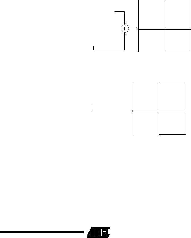
Program execution continues at address contained by the Z-register (i.e., the PC is loaded with the contents of the Z-register).
Relative Program Addressing, Figure 19. Relative Program Memory Addressing |
|||||
RJMP and RCALL |
|
|
PROGRAM MEMORY |
||
|
|
|
|
||
|
|
|
|
$000 |
|
|
|
|
|||
15 |
0 |
|
|
|
|
|
|
|
|
|
|
|
|
PC |
|
|
|
|
|
|
|
|
|
15 |
12 |
11 |
0 |
|
|
|
OP |
|
k |
|
|
|
|
|
$1FFF
Direct Program Addressing,
JMP and CALL
Memory Access Times
and Instruction
Execution Timing
1228B–09/01
Program execution continues at address PC + k + 1. The relative address k is -2048 to 2047.
Figure 20. Direct Program Addressing
PROGRAM MEMORY
$0000
31 |
21 20 |
16 |
||
|
|
OP |
|
|
|
|
|
|
|
|
|
16 LSBs |
|
|
|
|
|
|
|
15 |
|
|
0 |
|
$1FFF
Program execution continues at the address immediate in the instruction words.
This section describes the general access timing concepts for instruction execution and internal memory access.
The AVR CPU is driven by the System Clock Ø, directly generated from the external clock crystal for the chip. No internal clock division is used.
Figure 21 shows the parallel instruction fetches and instruction executions enabled by the Harvard architecture and the fast-access register file concept. This is the basic pipelining concept to obtain up to 1 MIPS per MHz with the corresponding unique results for functions per cost, functions per clocks and functions per power unit.
17
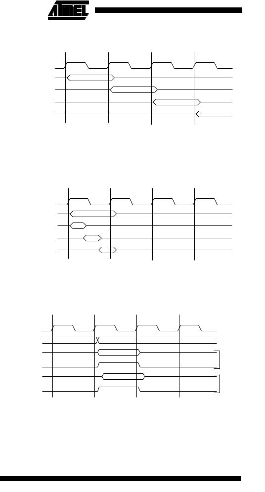
Figure 21. The Parallel Instruction Fetches and Instruction Executions
T1 |
T2 |
T3 |
T4 |
System Clock Ø
1st Instruction Fetch
1st Instruction Execute 2nd Instruction Fetch 2nd Instruction Execute 3rd Instruction Fetch 3rd Instruction Execute 4th Instruction Fetch
Figure 22 shows the internal timing concept for the register file. In a single clock cycle an ALU operation using two register operands is executed and the result is stored back to the destination register.
Figure 22. Single Cycle ALU Operation
T1 |
T2 |
T3 |
T4 |
System Clock Ø
Total Execution Time
Register Operands Fetch
ALU Operation Execute
Result Write Back
The internal data SRAM access is performed in two System Clock cycles as described in Figure 23.
Figure 23. On-chip Data SRAM Access Cycles
T1 |
T2 |
T3 |
T4 |
System Clock Ø
Address |
Prev. Address |
Address |
Data
WR
Data
RD
Read Write
18 ATmega161(L)
1228B–09/01

 ATmega161(L)
l/O Memory
The I/O space definition of the ATmega161 is shown in Table 1.
Table 1. |
ATmega161 I/O Space(1) |
||
I/O Address |
|
|
|
(SRAM Address) |
Name |
Function |
|
|
|
|
|
$3F($5F) |
SREG |
Status REGister |
|
|
|
|
|
$3E |
($5E) |
SPH |
Stack Pointer High |
|
|
|
|
$3D |
($5D) |
SPL |
Stack Pointer Low |
|
|
|
|
$3B |
($5B) |
GIMSK |
General Interrupt MaSK register |
|
|
|
|
$3A |
($5A) |
GIFR |
General Interrupt Flag Register |
|
|
|
|
$39 |
($59) |
TIMSK |
Timer/Counter Interrupt MaSK Register |
|
|
|
|
$38 |
($58) |
TIFR |
Timer/Counter Interrupt Flag Register |
|
|
|
|
$37 |
($57) |
SPMCR |
Store Program Memory Control Register |
|
|
|
|
$36 |
($56) |
EMCUCR |
Extended MCU general Control Register |
|
|
|
|
$35 |
($55) |
MCUCR |
MCU general Control Register |
|
|
|
|
$34 |
($54) |
MCUSR |
MCU general Status Register |
|
|
|
|
$33 |
($53) |
TCCR0 |
Timer/Counter0 Control Register |
|
|
|
|
$32 |
($52) |
TCNT0 |
Timer/Counter0 (8-bit) |
|
|
|
|
$31 |
($51) |
OCR0 |
Timer/Counter0 Output Compare Register |
|
|
|
|
$30 |
($50) |
SFIOR |
Special Function IO Register |
|
|
|
|
$2F |
($4F) |
TCCR1A |
Timer/Counter1 Control Register A |
|
|
|
|
$2E |
($4E) |
TCCR1B |
Timer/Counter1 Control Register B |
|
|
|
|
$2D |
($4D) |
TCNT1H |
Timer/Counter1 High Byte |
|
|
|
|
$2C |
($4C) |
TCNT1L |
Timer/Counter1 Low Byte |
|
|
|
|
$2B |
($4B) |
OCR1AH |
Timer/Counter1 Output Compare RegisterA High Byte |
|
|
|
|
$2A |
($4A) |
OCR1AL |
Timer/Counter1 Output Compare RegisterA Low Byte |
|
|
|
|
$29 |
($49) |
OCR1BH |
Timer/Counter1 Output Compare RegisterB High Byte |
|
|
|
|
$28 |
($48) |
OCR1BL |
Timer/Counter1 Output Compare RegisterB Low Byte |
|
|
|
|
$27 |
($47) |
TCCR2 |
Timer/Counter2 Control Register |
|
|
|
|
$26 |
($46) |
ASSR |
Asynchronous mode StatuS Register |
|
|
|
|
$25 |
($45) |
ICR1H |
Timer/Counter1 Input Capture Register High Byte |
|
|
|
|
$24 |
($44) |
ICR1L |
Timer/Counter1 Input Capture Register Low Byte |
|
|
|
|
$23 |
($43) |
TCNT2 |
Timer/Counter2 (8-bit) |
|
|
|
|
$22 |
($42) |
OCR2 |
Timer/Counter2 Output Compare Register |
|
|
|
|
$21 |
($41) |
WDTCR |
Watchdog Timer Control Register |
|
|
|
|
$20 |
($40) |
UBRRHI |
UART Baud Register HIgh |
|
|
|
|
$1F |
($3F) |
EEARH |
EEPROM Address Register High |
|
|
|
|
$1E |
($3E) |
EEARL |
EEPROM Address Register Low |
|
|
|
|
$1D |
($3D) |
EEDR |
EEPROM Data Register |
|
|
|
|
19
1228B–09/01
|
|
|
|
|
|
|
|
|
|
|
|
|
|
|
|
|
|
|
|
|
|
|
|
|
|
|
|
Table 1. |
ATmega161 I/O Space(1) (Continued) |
|||||
I/O Address |
|
|
|
|
|
|
(SRAM Address) |
Name |
|
|
Function |
||
|
|
|
|
|
|
|
$1C |
($3C) |
EECR |
|
|
EEPROM Control Register |
|
|
|
|
|
|
||
$1B($3B) |
PORTA |
|
|
Data Register, Port A |
||
|
|
|
|
|
|
|
$1A |
($3A) |
DDRA |
|
|
Data Direction Register, Port A |
|
|
|
|
|
|
|
|
$19 |
($39) |
PINA |
|
|
Input Pins, Port A |
|
|
|
|
|
|
|
|
$18 |
($38) |
PORTB |
|
|
Data Register, Port B |
|
|
|
|
|
|
|
|
$17 |
($37) |
DDRB |
|
|
Data Direction Register, Port B |
|
|
|
|
|
|
|
|
$16 |
($36) |
PINB |
|
|
Input Pins, Port B |
|
|
|
|
|
|
|
|
$15 |
($35) |
PORTC |
|
|
Data Register, Port C |
|
|
|
|
|
|
|
|
$14 |
($34) |
DDRC |
|
|
Data Direction Register, Port C |
|
|
|
|
|
|
|
|
$13 |
($33) |
PINC |
|
|
Input Pins, Port C |
|
|
|
|
|
|
|
|
$12 |
($32) |
PORTD |
|
|
Data Register, Port D |
|
|
|
|
|
|
|
|
$11 |
($31) |
DDRD |
|
|
Data Direction Register, Port D |
|
|
|
|
|
|
|
|
$10 |
($30) |
PIND |
|
|
Input Pins, Port D |
|
|
|
|
|
|
|
|
$0F |
($2F) |
SPDR |
|
|
SPI I/O Data Register |
|
|
|
|
|
|
|
|
$0E |
($2E) |
SPSR |
|
|
SPI Status Register |
|
|
|
|
|
|
|
|
$0D |
($2D) |
SPCR |
|
|
SPI Control Register |
|
|
|
|
|
|
|
|
$0C |
($2C) |
UDR0 |
|
|
UART0 I/O Data Register |
|
|
|
|
|
|
|
|
$0B |
($2B) |
UCSR0A |
|
|
UART0 Control and Status Register |
|
|
|
|
|
|
|
|
$0A |
($2A) |
UCSR0B |
|
|
UART0 Control and Status Register |
|
|
|
|
|
|
|
|
$09 |
($29) |
UBRR0 |
|
|
UART0 Baud Rate Register |
|
|
|
|
|
|
|
|
$08 |
($28) |
ACSR |
|
|
Analog Comparator Control and Status Register |
|
|
|
|
|
|
|
|
$07 |
($27) |
PORTE |
|
|
Data Register, Port E |
|
|
|
|
|
|
|
|
$06 |
($26) |
DDRE |
|
|
Data Direction Register, Port E |
|
|
|
|
|
|
|
|
$05 |
($25) |
PINE |
|
|
Input Pins, Port E |
|
|
|
|
|
|
|
|
$03 |
($23) |
UDR1 |
|
|
UART1 I/O Data Register |
|
|
|
|
|
|
|
|
$02 |
($22) |
UCSR1A |
|
|
UART1 Control and Status Register |
|
|
|
|
|
|
|
|
$01 |
($21) |
UCSR1B |
|
|
UART1 Control and Status Register |
|
|
|
|
|
|
|
|
$00 |
($20) |
UBRR1 |
|
|
UART1 Baud Rate Register |
|
|
|
|
|
|
|
|
Note: 1. Reserved and unused locations are not shown in this table.
20 ATmega161(L)
1228B–09/01