Материал: DOC1228

 ATmega161(L)
All ATmega161 I/Os and peripherals are placed in the I/O space. The I/O locations are accessed by the IN and OUT instructions transferring data between the 32 general purpose working registers and the I/O space. I/O registers within the address range $00 - $1F are directly bit-accessible using the SBI and CBI instructions. In these registers, the value of single bits can be checked by using the SBIS and SBIC instructions. Refer to the instruction set section for more details. When using the I/O specific commands IN and OUT, the I/O addresses $00 - $3F must be used. When addressing I/O registers as SRAM, $20 must be added to this address. All I/O register addresses throughout this document are shown with the SRAM address in parentheses.
For compatibility with future devices, reserved bits should be written to zero if accessed.
Reserved I/O memory addresses should never be written.
Some of the status flags are cleared by writing a logical “1” to them. Note that the CBI and SBI instructions will operate on all bits in the I/O register, writing a one back into any flag read as set, thus clearing the flag. The CBI and SBI instructions work with registers $00 to $1F only.
The I/O and peripherals control registers are explained in the following sections.
Status Register – SREG |
The AVR status register (SREG) at I/O space location $3F ($5F) is defined as: |
|
|||||||||
|
Bit |
7 |
6 |
5 |
4 |
3 |
2 |
1 |
0 |
|
|
|
|
|
|
|
|
|
|
|
|
|
|
|
$3F ($5F) |
I |
T |
H |
S |
V |
N |
Z |
C |
SREG |
|
|
|
|
|
|
|
|
|
|
|
|
|
|
Read/Write |
R/W |
R/W |
R/W |
R/W |
R/W |
R/W |
R/W |
R/W |
|
|
|
Initial Value |
0 |
0 |
0 |
0 |
0 |
0 |
0 |
0 |
|
|
• Bit 7 – I: Global Interrupt Enable
The global interrupt enable bit must be set (one) for the interrupts to be enabled. The individual interrupt enable control is then performed in separate control registers. If the global interrupt enable bit is cleared (zero), none of the interrupts are enabled independent of the individual interrupt enable settings. The I-bit is cleared by hardware after an interrupt has occurred and is set by the RETI instruction to enable subsequent interrupts.
• Bit 6 – T: Bit Copy Storage
The bit copy instructions BLD (Bit LoaD) and BST (Bit STore) use the T-bit as source and destination for the operated bit. A bit from a register in the register file can be copied into T by the BST instruction and a bit in T can be copied into a bit in a register in the register file by the BLD instruction.
• Bit 5 – H: Half-carry Flag
The half-carry flag H indicates a half carry in some arithmetic operations. See the Instruction Set description for detailed information.
• Bit 4 – S: Sign Bit, S = N V
The S-bit is always an exclusive or between the negative flag N and the two’s complement overflow flag V. See the Instruction Set description for detailed information.
• Bit 3 – V: Two’s Complement Overflow Flag
The two’s complement overflow flag V supports two’s complement arithmetics. See the
Instruction Set Description for detailed information.
• Bit 2 – N: Negative Flag
The negative flag N indicates a negative result after the different arithmetic and logic operations. See the Instruction Set description for detailed information.
21
1228B–09/01

Stack Pointer – SP
Reset and Interrupt
Handling
• Bit 1 – Z: Zero Flag
The zero flag Z indicates a zero result after the different arithmetic and logic operations. See the Instruction Set description for detailed information.
• Bit 0 – C: Carry Flag
The carry flag C indicates a carry in an arithmetic or logic operation. See the Instruction Set description for detailed information.
Note that the status register is not automatically stored when entering an interrupt routine and restored when returning from an interrupt routine. This must be handled by software.
The ATmega161 Stack Pointer is implemented as two 8-bit registers in the I/O space locations $3E ($5E) and $3D ($5D). As the ATmega161 supports up to 64-Kbyte memory, all 16 bits are used.
Bit |
15 |
14 |
13 |
12 |
11 |
10 |
9 |
8 |
|
$3E ($5E) |
SP15 |
SP14 |
SP13 |
SP12 |
SP11 |
SP10 |
SP9 |
SP8 |
SPH |
|
|
|
|
|
|
|
|
|
|
$3D ($5D) |
SP7 |
SP6 |
SP5 |
SP4 |
SP3 |
SP2 |
SP1 |
SP0 |
SPL |
|
|
|
|
|
|
|
|
|
|
|
7 |
6 |
5 |
4 |
3 |
2 |
1 |
0 |
|
Read/Write |
R/W |
R/W |
R/W |
R/W |
R/W |
R/W |
R/W |
R/W |
|
|
R/W |
R/W |
R/W |
R/W |
R/W |
R/W |
R/W |
R/W |
|
Initial Value |
0 |
0 |
0 |
0 |
0 |
0 |
0 |
0 |
|
|
0 |
0 |
0 |
0 |
0 |
0 |
0 |
0 |
|
The Stack Pointer points to the data SRAM stack area where the Subroutine and Interrupt stacks are located. This Stack space in the data SRAM must be defined by the program before any subroutine calls are executed or interrupts are enabled. The Stack Pointer must be set to point above $60. The Stack Pointer is decremented by 1 when data is pushed onto the Stack with the PUSH instruction, and it is decremented by 2 when an address is pushed onto the Stack with subroutine calls and interrupts. The Stack Pointer is incremented by 1 when data is popped from the Stack with the POP instruction, and it is incremented by 2 when an address is popped from the Stack with return from subroutine RET or return from interrupt (RETI).
The ATmega161 provides 20 different interrupt sources. These interrupts and the separate reset vector each have a separate program vector in the program memory space. All interrupts are assigned individual enable bits that must be set (one) together with the I-bit in the status register in order to enable the interrupt.
The lowest addresses in the program memory space are automatically defined as the Reset and Interrupt vectors. The complete list of vectors is shown in Table 2. The list also determines the priority levels of the different interrupts. The lower the address, the higher the priority level. RESET has the highest priority, and next is INT0 (the External Interrupt Request 0) and so on.
22 ATmega161(L)
1228B–09/01

|
|
|
|
|
|
ATmega161(L) |
|
|
|
|
|
|
|
|
|
Table 2. Reset and Interrupt Vectors(1) |
|
|||
|
|
|
|
|||
|
|
|
|
|||
|
|
Vector |
|
|
|
|
|
|
No. |
Program Address |
Source |
Interrupt Definition |
|
|
|
|
|
|
||
|
|
1 |
$000 |
RESET |
External Pin, Power-on Reset, Brown-out |
|
|
|
|
|
|
Reset and Watchdog Reset |
|
|
|
|
|
|
||
|
|
2 |
$002 |
INT0 |
External Interrupt Request 0 |
|
|
|
|
|
|
||
|
|
3 |
$004 |
INT1 |
External Interrupt Request 1 |
|
|
|
|
|
|
||
|
|
4 |
$006 |
INT2 |
External Interrupt Request 2 |
|
|
|
|
|
|
||
|
|
5 |
$008 |
TIMER2 COMP |
Timer/Counter2 Compare Match |
|
|
|
|
|
|
||
|
|
6 |
$00a |
TIMER2 OVF |
Timer/Counter2 Overflow |
|
|
|
|
|
|
||
|
|
7 |
$00c |
TIMER1 CAPT |
Timer/Counter1 Capture Event |
|
|
|
|
|
|
||
|
|
8 |
$00e |
TIMER1 COMPA |
Timer/Counter1 Compare Match A |
|
|
|
|
|
|
||
|
|
9 |
$010 |
TIMER1 COMPB |
Timer/Counter1 Compare Match B |
|
|
|
|
|
|
||
|
|
10 |
$012 |
TIMER1 OVF |
Timer/Counter1 Overflow |
|
|
|
|
|
|
||
|
|
11 |
$014 |
TIMER0 COMP |
Timer/Counter0 Compare Match |
|
|
|
|
|
|
||
|
|
12 |
$016 |
TIMER0 OVF |
Timer/Counter0 Overflow |
|
|
|
|
|
|
||
|
|
13 |
$018 |
SPI, STC |
Serial Transfer Complete |
|
|
|
|
|
|
||
|
|
14 |
$01a |
UART0, RX |
UART0, Rx Complete |
|
|
|
|
|
|
||
|
|
15 |
$01c |
UART1, RX |
UART1, Rx Complete |
|
|
|
|
|
|
||
|
|
16 |
$01e |
UART0, UDRE |
UART0 Data Register Empty |
|
|
|
|
|
|
||
|
|
17 |
$020 |
UART1, UDRE |
UART1 Data Register Empty |
|
|
|
|
|
|
||
|
|
18 |
$022 |
UART0, TX |
UART0, Tx Complete |
|
|
|
|
|
|
||
|
|
19 |
$024 |
UART1, TX |
UART1, Tx Complete |
|
|
|
|
|
|
||
|
|
20 |
$026 |
EE_RDY |
EEPROM Ready |
|
|
|
|
|
|
||
|
|
21 |
$028 |
ANA_COMP |
Analog Comparator |
|
|
|
|
|
|
|
|
Note: 1. If BOOTRST fuse is programmed, the reset vector is located on program address $1e00, see Table 39 on page 110 for details.
The most typical and general program setup for the Reset and Interrupt vector addresses are:
Address Labels |
Code |
|
Comments |
|
$000 |
jmp |
RESET |
; Reset Handler |
|
$002 |
jmp |
EXT_INT0 |
; IRQ0 Handler |
|
$004 |
jmp |
EXT_INT1 |
; IRQ1 Handler |
|
$006 |
jmp |
EXT_INT2 |
; IRQ2 Handler |
|
$008 |
jmp |
TIM2_COMP |
; Timer2 |
Compare Handler |
$00a |
jmp |
TIM2_OVF |
; Timer2 |
Overflow Handler |
$00c |
jmp |
TIM1_CAPT |
; Timer1 |
Capture Handler |
$00e |
jmp |
TIM1_COMPA |
; Timer1 |
CompareA Handler |
$010 |
jmp |
TIM1_COMPB |
; Timer1 |
CompareB Handler |
$012 |
jmp |
TIM1_OVF |
; Timer1 Overflow Handler |
|
$014 |
jmp |
TIM0_COMP |
; Timer0 |
Compare Handler |
$016 |
jmp |
TIM0_OVF |
; Timer0 |
Overflow Handler |
$018 |
jmp |
SPI_STC; |
; SPI Transfer Complete Handler |
|
23
1228B–09/01

|
|
|
|
|
|
|
|
|
|
|
|
|
|
|
|
|
|
|
|
|
|
|
|
|
|
|
|
|
|
|
|
|
|
|
|
|
|
|
|
$01a |
|
jmp |
UART_RXC0 |
; |
UART0 RX Complete Handler |
||||
$01c |
|
jmp |
UART_RXC1 |
; |
UART1 RX Complete Handler |
||||
$01e |
|
jmp |
UART_DRE0 |
; |
UDR0 Empty Handler |
||||
$020 |
|
jmp |
UART_DRE1 |
; |
UDR1 Empty Handler |
||||
$022 |
|
jmp |
UART_TXC0 |
; |
UART0 TX Complete Handler |
||||
$024 |
|
jmp |
UART_TXC1 |
; |
UART1 TX Complete Handler |
||||
$026 |
|
jmp |
EE_RDY |
; |
EEPROM Ready Handler |
||||
$028 |
|
jmp |
ANA_COMP |
; |
Analog Comparator Handler |
||||
; |
|
|
|
|
|
|
|
|
|
$02a |
MAIN: |
ldi r16,high(RAMEND) ; |
Main program start |
||||||
$02b |
|
out SPH,r16 |
|
|
|||||
$02c |
|
ldi r16,low(RAMEND) |
|
|
|||||
$02d |
|
out SPL,r16 |
|
|
|||||
$02e |
|
<instr> |
xxx |
|
|
||||
… |
… |
… |
… |
|
|
||||
When the BOOTRST fuse is programmed, the most typical and general program setup for the Reset and Interrupt vector addresses are:
Address |
Labels |
Code |
|
Comments |
|
.org $002 |
|
|
|
; Reset is located at $1e000 |
|
$002 |
|
jmp |
EXT_INT0 |
; IRQ0 Handler |
|
$004 |
|
jmp |
EXT_INT1 |
; IRQ1 Handler |
|
$006 |
|
jmp |
EXT_INT2 |
; IRQ2 Handler |
|
$008 |
|
jmp |
TIM2_COMP |
; Timer2 |
Compare Handler |
$00a |
|
jmp |
TIM2_OVF |
; Timer2 |
Overflow Handler |
$00c |
|
jmp |
TIM1_CAPT |
; Timer1 |
Capture Handler |
$00e |
|
jmp |
TIM1_COMPA |
; Timer1 |
CompareA Handler |
$010 |
|
jmp |
TIM1_COMPB |
; Timer1 |
CompareB Handler |
$012 |
|
jmp |
TIM1_OVF |
; Timer1 |
Overflow Handler |
$014 |
|
jmp |
TIM0_COMP |
; Timer0 |
Compare Handler |
$016 |
|
jmp |
TIM0_OVF |
; Timer0 |
Overflow Handler |
$018 |
|
jmp |
SPI_STC; |
; SPI Transfer Complete Handler |
|
$01a |
|
jmp |
UART_RXC0 |
; UART0 RX Complete Handler |
|
$01c |
|
jmp |
UART_RXC1 |
; UART1 RX Complete Handler |
|
$01e |
|
jmp |
UART_DRE0 |
; UDR0 Empty Handler |
|
$020 |
|
jmp |
UART_DRE1 |
; UDR1 Empty Handler |
|
$022 |
|
jmp |
UART_TXC0 |
; UART0 TX Complete Handler |
|
$024 |
|
jmp |
UART_TXC1 |
; UART1 TX Complete Handler |
|
$026 |
|
jmp |
EE_RDY |
; EEPROM |
Ready Handler |
$028 |
|
jmp |
ANA_COMP |
; Analog |
Comparator Handler |
; |
|
|
|
|
|
$02a |
MAIN: |
ldi r16,high(RAMEND); Main program start |
|||
$02b |
|
out SPH,r16 |
|
|
|
$02c |
|
ldi r16,low(RAMEND) |
|
|
|
$02d |
|
out SPL,r16 |
|
|
|
$02e |
|
<instr> |
xxx |
|
|
; |
|
|
|
|
|
.org $1e00 |
|
|
|
|
|
$1e00 |
|
jmp |
RESET |
; Reset handler |
|
… |
… |
… |
… |
|
|
24 ATmega161(L)
1228B–09/01
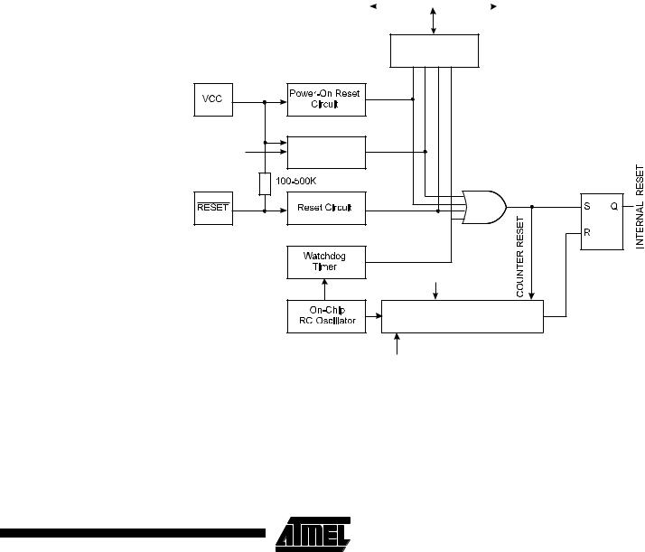
 ATmega161(L)
Reset Sources |
The ATmega161 has four sources of reset: |
||||
|
• Power-on Reset. The MCU is reset when the supply voltage is below the Power-on |
||||
|
Reset threshold (VPOT). |
||||
|
• External Reset. The MCU is reset when a low level is present on the |
|
pin for |
||
|
RESET |
||||
|
more than 500 ns. |
||||
|
• Watchdog Reset. The MCU is reset when the Watchdog timer period expires and |
||||
|
the Watchdog is enabled. |
||||
|
• Brown-out Reset. The MCU is reset when the supply voltage VCC falls below a |
||||
|
certain voltage. |
||||
|
During reset, all I/O registers are then set to their initial values and the program starts |
||||
|
execution from address $000. The instruction placed in address $000 must be a JMP |
||||
|
(relative jump) instruction to the reset handling routine. If the program never enables an |
||||
|
interrupt source, the interrupt vectors are not used and regular program code can be |
||||
|
placed at these locations. The circuit diagram in Figure 24 shows the reset logic. Table 3 |
||||
|
and Table 4 define the timing and electrical parameters of the reset circuitry |
||||
|
Figure 24. Reset Logic |
||||
|
|
DATA BUS |
|
||
MCU Status
Register (MCUSR)
WDRF |
BORF |
EXTRF |
PORF |
BODEN
Brown-Out
BODLEVEL  Reset Circuit
CKSEL[2:0]
Delay Counters
Full
CK
25
1228B–09/01