Материал: DOC1228
ATmega161(L)
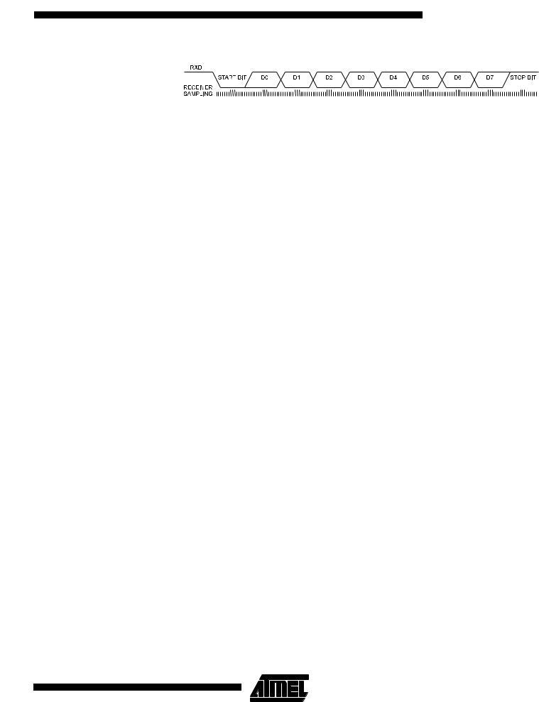
Figure 47. Sampling Received Data(1)
Note: 1. This figure is not valid when the UART speed is doubled. See “Double-speed
Transmission” on page 77 for a detailed description.
|
When the stop bit enters the receiver, the majority of the three samples must be one to |
|
accept the stop bit. If two or more samples are logical “0”s, the Framing Error (FEn) flag |
|
in the UART Control and Status Register (UCSRnA) is set. Before reading the UDRn |
|
register, the user should always check the FEn bit to detect framing errors. |
|
Whether or not a valid stop bit is detected at the end of a character reception cycle, the |
|
data is transferred to UDRn and the RXCn flag in UCSRnA is set. UDRn is in fact two |
|
physically separate registers, one for transmitted data and one for received data. When |
|
UDRn is read, the Receive Data register is accessed, and when UDRn is written, the |
|
Transmit Data register is accessed. If 9-bit data word is selected (the CHR9n bit in the |
|
UART Control and Status Register [UCSRnB] is set), the RXB8n bit in UCSRnB is |
|
loaded with bit 9 in the Transmit shift register when data is transferred to UDRn. |
|
If, after having received a character, the UDRn register has not been read since the last |
|
receive, the OverRun (ORn) flag in UCSRnB is set. This means that the last data byte |
|
shifted into the shift register could not be transferred to UDRn and has been lost. The |
|
ORn bit is buffered and is updated when the valid data byte in UDRn is read. Thus, the |
|
user should always check the ORn bit after reading the UDRn register in order to detect |
|
any overruns if the baud rate is high or CPU load is high. |
|
When the RXEN bit in the UCSRnB register is cleared (zero), the receiver is disabled. |
|
This means that the PD0 pin can be used as a general I/O pin. When RXEN is set, the |
|
UART receiver will be connected to PD0 (UART0) or PB2 (UART1), which is forced to |
|
be an input pin regardless of the setting of the DDD0 in DDRD (UART0) or DDB2 bit in |
|
DDRB (UART1). When PD0 (UART0) or PB2 (UART1) is forced to input by the UART, |
|
the PORTD0 (UART0) or PORTB2 (UART1) bit can still be used to control the pull-up |
|
resistor on the pin. |
|
Note that PB2 (UART1) also is used as one of the input pins to the Analog Comparator. |
|
It is therefore not recommended to use UART1 if the Analog Comparator also is used in |
|
the application at the same time. |
|
When the CHR9n bit in the UCSRnB register is set, transmitted and received characters |
|
are nine bits long plus start and stop bits. The ninth data bit to be transmitted is the |
|
TXB8n bit in UCSRnB register. This bit must be set to the wanted value before a trans- |
|
mission is initiated by writing to the UDRn register. The ninth data bit received is the |
|
RXB8n bit in the UCSRnB register. |
Multi-processor |
The Multi-processor Communication Mode enables several slave MCUs to receive data |
Communication Mode |
from a master MCU. This is done by first decoding an address byte to find out which |
|
MCU has been addressed. If a particular slave MCU has been addressed, it will receive |
|
the following data bytes as normal, while the other slave MCUs will ignore the data bytes |
|
until another address byte is received. |
|
For an MCU to act as a master MCU, it should enter 9-bit transmission mode (CHR9n in |
|
UCSRnB set). The ninth bit must be one to indicate that an address byte is being trans- |
|
mitted, and zero to indicate that a data byte is being transmitted. |
71
1228B–09/01
UART Control
UART0 I/O Data Register –
UDR0
UART1 I/O Data Register –
UDR1
UART0 Control and Status
Registers – UCSR0A
UART1 Control and Status
Registers – UCSR1A
For the slave MCUs, the mechanism appears slightly different for 8-bit and 9-bit reception mode. In 8-bit reception mode (CHR9n in UCSRnB cleared), the stop bit is one for an address byte and zero for a data byte. In 9-bit reception mode (CHR9n in UCSRnB set), the ninth bit is one for an address byte and zero for a data byte, whereas the stop bit is always high.
The following procedure should be used to exchange data in Multi-processor Communication Mode:
1.All slave MCUs are in Multi-processor Communication Mode (MPCMn in UCSRnA is set).
2.The master MCU sends an address byte and all slaves receive and read this byte. In the slave MCUs, the RXCn flag in UCSRnA will be set as normal.
3.Each slave MCU reads the UDRn register and determines if it has been selected. If so, it clears the MPCMn bit in UCSRnA; otherwise, it waits for the next address byte.
4.For each received data byte, the receiving MCU will set the receive complete flag (RXCn in UCSRnA). In 8-bit mode, the receiving MCU will also generate a framing error (FEn in UCSRnA set), since the stop bit is zero. The other slave MCUs, which still have the MPCMn bit set, will ignore the data byte. In this case, the UDRn register and the RXCn, FEn, or flags will not be affected.
5.After the last byte has been transferred, the process repeats from step 2.
Bit |
7 |
6 |
5 |
4 |
3 |
2 |
1 |
0 |
|
$0C ($2C) |
MSB |
|
|
|
|
|
|
LSB |
UDR0 |
|
|
|
|
|
|
|
|
|
|
Read/Write |
R/W |
R/W |
R/W |
R/W |
R/W |
R/W |
R/W |
R/W |
|
Initial Value |
0 |
0 |
0 |
0 |
0 |
0 |
0 |
0 |
|
Bit |
7 |
6 |
5 |
4 |
3 |
2 |
1 |
0 |
|
|
|
|
|
|
|
|
|
|
|
$03 ($23) |
MSB |
|
|
|
|
|
|
LSB |
UDR1 |
|
|
|
|
|
|
|
|
|
|
Read/Write |
R/W |
R/W |
R/W |
R/W |
R/W |
R/W |
R/W |
R/W |
|
Initial Value |
0 |
0 |
0 |
0 |
0 |
0 |
0 |
0 |
|
The UDRn register is actually two physically separate registers sharing the same I/O address. When writing to the register, the UART Transmit Data register is written. When reading from UDRn, the UART Receive Data register is read.
Bit |
7 |
6 |
5 |
4 |
3 |
2 |
1 |
0 |
|
$0B ($2B) |
RXC0 |
TXC0 |
UDRE0 |
FE0 |
OR0 |
– |
U2X0 |
MPCM0 |
UCSR0A |
|
|
|
|
|
|
|
|
|
|
Read/Write |
R |
R/W |
R |
R |
R |
R |
R/W |
R/W |
|
Initial Value |
0 |
0 |
1 |
0 |
0 |
0 |
0 |
0 |
|
Bit |
7 |
6 |
5 |
4 |
3 |
2 |
1 |
0 |
|
|
|
|
|
|
|
|
|
|
|
$02 ($22) |
RXC1 |
TXC1 |
UDRE1 |
FE1 |
OR1 |
– |
U2X1 |
MPCM1 |
UCSR1A |
|
|
|
|
|
|
|
|
|
|
Read/Write |
R |
R/W |
R |
R |
R |
R |
R/W |
R/W |
|
Initial Value |
0 |
0 |
1 |
0 |
0 |
0 |
0 |
0 |
|
72 ATmega161(L)
1228B–09/01

ATmega161(L)
• Bit 7 – RXC0/RXC1: UART Receive Complete
This bit is set (one) when a received character is transferred from the Receiver Shift register to UDRn. The bit is set regardless of any detected framing errors. When the RXCIEn bit in UCSRnB is set, the UART Receive Complete interrupt will be executed when RXCn is set (one). RXCn is cleared by reading UDRn. When interrupt-driven data reception is used, the UART Receive Complete Interrupt routine must read UDRn in order to clear RXCn; otherwise, a new interrupt will occur once the interrupt routine terminates.
• Bit 6 – TXC0/TXC1: UART Transmit Complete
This bit is set (one) when the entire character (including the stop bit) in the Transmit shift register has been shifted out and no new data has been written to UDRn. This flag is especially useful in half-duplex communications interfaces, where a transmitting application must enter receive mode and free the communications bus immediately after completing the transmission.
When the TXCIEn bit in UCSRnB is set, setting of TXCn causes the UART Transmit Complete interrupt to be executed. TXCn is cleared by hardware when executing the corresponding interrupt handling vector. Alternatively, the TXCn bit is cleared (zero) by writing a logical “1” to the bit.
• Bit 5 – UDRE0/UDRE1: UART Data Register Empty
This bit is set (one) when a character written to UDRn is transferred to the Transmit shift register. Setting of this bit indicates that the transmitter is ready to receive a new character for transmission.
When the UDRIEn bit in UCSRnB is set, the UART Transmit Complete interrupt will be executed as long as UDREn is set and the global interrupt enable bit in SREG is set. UDREn is cleared by writing UDRn. When interrupt-driven data transmittal is used, the UART Data Register Empty Interrupt routine must write UDRn in order to clear UDREn, otherwise a new interrupt will occur once the interrupt routine terminates.
UDREn is set (one) during reset to indicate that the transmitter is ready.
• Bit 4 – FE0/FE1: Framing Error
This bit is set if a Framing Error condition is detected, i.e., when the stop bit of an incoming character is zero.
The FEn bit is cleared when the stop bit of received data is one.
• Bit 3 – OR0/OR1: OverRun
This bit is set if an Overrun condition is detected, i.e., when a character already present in the UDRn register is not read before the next character has been shifted into the Receiver Shift register. The ORn bit is buffered, which means that it will be set once the valid data still in UDRn is read.
The ORn bit is cleared (zero) when data is received and transferred to UDRn.
• Bit 2 – Res: Reserved Bit
This bit is reserved bit in the ATmega161 and will always read as zero.
• Bit 1 – U2X0/U2X1: Double the UART Transmission Speed
When this bit is set (one), the UART speed will be doubled. This means that a bit will be transmitted/received in 8 CPU clock periods instead of 16 CPU clock periods. For a detailed description, see “Double-speed Transmission” on page 77.
73
1228B–09/01
UART0 Control and Status
Registers – UCSR0B
UART1 Control and Status
Registers – UCSR1B
• Bit 0 – MPCM0/MPCM1: Multi-processor Communication Mode
This bit is used to enter Multi-processor Communication Mode. The bit is set when the slave MCU waits for an address byte to be received. When the MCU has been addressed, the MCU switches off the MPCMn bit and starts data reception.
For a detailed description, see “Multi-processor Communication Mode”.
Bit |
7 |
6 |
5 |
4 |
3 |
2 |
1 |
0 |
|
$0A ($2A) |
RXCIE0 |
TXCIE0 |
UDRIE0 |
RXEN0 |
TXEN0 |
CHR90 |
RXB80 |
TXB80 |
UCSR0B |
|
|
|
|
|
|
|
|
|
|
Read/Write |
R/W |
R/W |
R/W |
R/W |
R/W |
R/W |
R |
R/W |
|
Initial Value |
0 |
0 |
0 |
0 |
0 |
0 |
1 |
0 |
|
Bit |
7 |
6 |
5 |
4 |
3 |
2 |
1 |
0 |
|
|
|
|
|
|
|
|
|
|
|
$01 ($21) |
RXCIE1 |
TXCIE1 |
UDRIE1 |
RXEN1 |
TXEN1 |
CHR91 |
RXB81 |
TXB81 |
UCSR1B |
|
|
|
|
|
|
|
|
|
|
Read/Write |
R/W |
R/W |
R/W |
R/W |
R/W |
R/W |
R |
R/W |
|
Initial Value |
0 |
0 |
0 |
0 |
0 |
0 |
1 |
0 |
|
• Bit 7 – RXCIE0/RXCIE1: RX Complete Interrupt Enable
When this bit is set (one), a setting of the RXCn bit in UCSRnA will cause the Receive Complete interrupt routine to be executed, provided that global interrupts are enabled.
• Bit 6 – TXCIE0/TXCIE1: TX Complete Interrupt Enable
When this bit is set (one), a setting of the TXCn bit in UCSRnA will cause the Transmit Complete interrupt routine to be executed, provided that global interrupts are enabled.
• Bit 5 – UDRIE0/UDREI1: UART Data Register Empty Interrupt Enable
When this bit is set (one), a setting of the UDREn bit in UCSRnA will cause the UART Data Register Empty interrupt routine to be executed, provided that global interrupts are enabled.
• Bit 4 – RXEN0/RXEN1: Receiver Enable
This bit enables the UART receiver when set (one). When the receiver is disabled, the TXCn, ORn and FEn status flags cannot become set. If these flags are set, turning off RXEN does not cause them to be cleared.
• Bit 3 – TXEN0/TXEN1: Transmitter Enable
This bit enables the UART transmitter when set (one). When disabling the transmitter while transmitting a character, the transmitter is not disabled before the character in the shift register plus any following character in UDRn has been completely transmitted.
• Bit 2 – CHR90/CHR91: 9-bit Characters
When this bit is set (one), transmitted and received characters are nine bits long, plus start and stop bits. The ninth bit is read and written by using the RXB8n and TXB8 bits in UCSRnB, respectively. The ninth data bit can be used as an extra stop bit or a parity bit.
• Bit 1 – RXB80/RXB81: Receive Data Bit 8
When CHR9n is set (one), RXB8n is the ninth data bit of the received character.
• Bit 0 – TXB80/TXB81: Transmit Data Bit 8
When CHR9n is set (one), TXB8n is the ninth data bit in the character to be transmitted.
74 ATmega161(L)
1228B–09/01

 ATmega161(L)
Baud Rate Generator
The baud rate generator is a frequency divider that generates baud rates according to the following equation:
BAUD fCK
= ---------------------------------
16(UBR + 1 )
•BAUD = Baud rate
•fCK= Crystal clock frequency
•UBR = Contents of the UBRRH and UBRR registers (0 - 4095)
•Note that this equation is not valid when the UART transmission speed is doubled. See “Double-speed Transmission” for a detailed description.
For standard crystal frequencies, the most commonly used baud rates can be generated by using the UBR settings in Table 24. UBR values that yield an actual baud rate differing less than 2% from the target baud rate are boldface in the table. However, using baud rates that have more than 1% error is not recommended. High error ratings give less noise resistance.
Table 24. UBR Settings at Various Crystal Frequencies
Baud Rate |
|
1 MHz |
%Error |
1.8432 MHz |
%Error |
|
2 MHz |
%Error |
2.4576 MHz |
%Error |
||
2400 |
UBR= |
25 |
0.2 |
UBR= |
47 |
0.0 |
UBR= |
51 |
0.2 |
UBR= |
63 |
0.0 |
4800 |
UBR= |
12 |
0.2 |
UBR= |
23 |
0.0 |
UBR= |
25 |
0.2 |
UBR= |
31 |
0.0 |
9600 |
UBR= |
6 |
7.5 |
UBR= |
11 |
0.0 |
UBR= |
12 |
0.2 |
UBR= |
15 |
0.0 |
14400 |
UBR= |
3 |
7.8 |
UBR= |
7 |
0.0 |
UBR= |
8 |
3.7 |
UBR= |
10 |
3.1 |
19200 |
UBR= |
2 |
7.8 |
UBR= |
5 |
0.0 |
UBR= |
6 |
7.5 |
UBR= |
7 |
0.0 |
28800 |
UBR= |
1 |
7.8 |
UBR= |
3 |
0.0 |
UBR= |
3 |
7.8 |
UBR= |
4 |
6.3 |
38400 |
UBR= |
1 |
22.9 |
UBR= |
2 |
0.0 |
UBR= |
2 |
7.8 |
UBR= |
3 |
0.0 |
57600 |
UBR= |
0 |
7.8 |
UBR= |
1 |
0.0 |
UBR= |
1 |
7.8 |
UBR= |
2 |
12.5 |
76800 |
UBR= |
0 |
22.9 |
UBR= |
1 |
33.3 |
UBR= |
1 |
22.9 |
UBR= |
1 |
0.0 |
115200 |
UBR= |
0 |
84.3 |
UBR= |
0 |
0.0 |
UBR= |
0 |
7.8 |
UBR= |
0 |
25.0 |
|
|
|
|
|
|
|
|
|
|
|||
Baud Rate |
3.2768 MHz |
%Error |
3.6864 MHz |
%Error |
|
4 MHz |
%Error |
4.608 MHz |
%Error |
|||
2400 |
UBR= |
84 |
0.4 |
UBR= |
95 |
0.0 |
UBR= |
103 |
0.2 |
UBR= |
119 |
0.0 |
4800 |
UBR= |
42 |
0.8 |
UBR= |
47 |
0.0 |
UBR= |
51 |
0.2 |
UBR= |
59 |
0.0 |
9600 |
UBR= |
20 |
1.6 |
UBR= |
23 |
0.0 |
UBR= |
25 |
0.2 |
UBR= |
29 |
0.0 |
14400 |
UBR= |
13 |
1.6 |
UBR= |
15 |
0.0 |
UBR= |
16 |
2.1 |
UBR= |
19 |
0.0 |
19200 |
UBR= |
10 |
3.1 |
UBR= |
11 |
0.0 |
UBR= |
12 |
0.2 |
UBR= |
14 |
0.0 |
28800 |
UBR= |
6 |
1.6 |
UBR= |
7 |
0.0 |
UBR= |
8 |
3.7 |
UBR= |
9 |
0.0 |
38400 |
UBR= |
4 |
6.3 |
UBR= |
5 |
0.0 |
UBR= |
6 |
7.5 |
UBR= |
7 |
6.7 |
57600 |
UBR= |
3 |
12.5 |
UBR= |
3 |
0.0 |
UBR= |
3 |
7.8 |
UBR= |
4 |
0.0 |
76800 |
UBR= |
2 |
12.5 |
UBR= |
2 |
0.0 |
UBR= |
2 |
7.8 |
UBR= |
3 |
6.7 |
115200 |
UBR= |
1 |
12.5 |
UBR= |
1 |
0.0 |
UBR= |
1 |
7.8 |
UBR= |
2 |
20.0 |
|
|
|
|
|
|
|
|
|
|
|||
Baud Rate |
7.3728 MHz |
%Error |
|
8 MHz |
%Error |
9.216 MHz |
%Error |
11.059 MHz |
%Error |
|||
2400 |
UBR= |
191 |
0.0 |
UBR= |
207 |
0.2 |
UBR= |
239 |
0.0 |
UBR= |
287 |
- |
4800 |
UBR= |
95 |
0.0 |
UBR= |
103 |
0.2 |
UBR= |
119 |
0.0 |
UBR= |
143 |
0.0 |
9600 |
UBR= |
47 |
0.0 |
UBR= |
51 |
0.2 |
UBR= |
59 |
0.0 |
UBR= |
71 |
0.0 |
14400 |
UBR= |
31 |
0.0 |
UBR= |
34 |
0.8 |
UBR= |
39 |
0.0 |
UBR= |
47 |
0.0 |
19200 |
UBR= |
23 |
0.0 |
UBR= |
25 |
0.2 |
UBR= |
29 |
0.0 |
UBR= |
35 |
0.0 |
28800 |
UBR= |
15 |
0.0 |
UBR= |
16 |
2.1 |
UBR= |
19 |
0.0 |
UBR= |
23 |
0.0 |
38400 |
UBR= |
11 |
0.0 |
UBR= |
12 |
0.2 |
UBR= |
14 |
0.0 |
UBR= |
17 |
0.0 |
57600 |
UBR= |
7 |
0.0 |
UBR= |
8 |
3.7 |
UBR= |
9 |
0.0 |
UBR= |
11 |
0.0 |
76800 |
UBR= |
5 |
0.0 |
UBR= |
6 |
7.5 |
UBR= |
7 |
6.7 |
UBR= |
8 |
0.0 |
115200 |
UBR= |
3 |
0.0 |
UBR= |
3 |
7.8 |
UBR= |
4 |
0.0 |
UBR= |
5 |
0.0 |
75
1228B–09/01