Материал: DOC1228
Using the External
Memory Interface
The interface consists of:
Port A: multiplexed low-order address bus and data bus
Port C: high-order address bus
The ALE pin: address latch enable
The RD and WR pin: read and write strobes
The external memory interface is enabled by setting the external SRAM enable bit (SRE) of the MCU control register (MCUCR) and will override the setting of the data direction registers DDRA, DDRD and DDRE. When the SRE bit is cleared (zero), the external memory interface is disabled and the normal pin and data direction settings are used. When SRE is low, the address space above the internal SRAM boundary is not mapped into the internal SRAM, as in AVR parts do not have an external memory interface.
When ALE goes from high to low, there is a valid address on Port A. ALE is low during a data transfer. RD and WR are active when accessing the external memory only.
When the external memory interface is enabled, the ALE signal may have short pulses when accessing the internal RAM, but the ALE signal is stable when accessing the external memory.
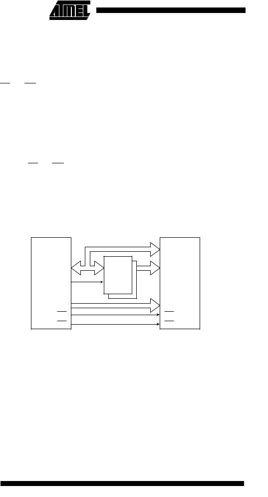
Figure 55 sketches how to connect an external SRAM to the AVR using eight latches that are transparent when G is high.
Figure 55. External SRAM Connected to the AVR
|
|
|
D[7:0] |
Port A |
D |
Q |
A[7:0] |
ALE |
G |
|
SRAM |
AVR |
|
|
|
|
|
|
|
Port C |
|
|
A[15:8] |
RD |
|
|
RD |
WR |
|
|
WR |
For details on the timing for the SRAM interface, please see Figure 84 through Figure 87 and Table 51 through Table 58.
86 ATmega161(L)
1228B–09/01

 ATmega161(L)
I/O Ports
All AVR ports have true read-modify-write functionality when used as general digital I/O ports. This means that the direction of one port pin can be changed without unintentionally changing the direction of any other pin with the SBI and CBI instructions. The same applies for changing drive value (if configured as output) or enabling/disabling of pull-up resistors (if configured as input).
Port A |
Port A is an 8-bit bi-directional I/O port. |
|
Three I/O memory address locations are allocated for the Port A, one each for the Data |
|
Register – PORTA, $1B($3B), Data Direction Register – DDRA, $1A($3A) and the Port |
|
A Input Pins – PINA, $19($39). The Port A Input Pins address is read-only, while the |
|
Data Register and the Data Direction Register are read/write. |
|
All port pins have individually selectable pull-up resistors. The Port A output buffers can |
|
sink 20 mA and thus drive LED displays directly. When pins PA0 to PA7 are used as |
|
inputs and are externally pulled low, they will source current if the internal pull-up resis- |
|
tors are activated. |
|
The Port A pins have alternate functions related to the optional external memory inter- |
|
face. Port A can be configured to be the multiplexed low-order address/data bus during |
|
accesses to the external data memory. In this mode, Port A has internal pull-up |
|
resistors. |
|
When Port A is set to the alternate function by the SRE (External SRAM Enable) bit in |
|
the MCUCR (MCU Control Register), the alternate settings override the Data Direction |
|
Register. |
Port A Data Register – PORTA
Port A Data Direction Register
– DDRA
Port A Input Pins Address –
PINA
Bit |
7 |
6 |
5 |
4 |
3 |
2 |
1 |
0 |
|
$1B ($3B) |
PORTA7 |
PORTA6 |
PORTA5 |
PORTA4 |
PORTA3 |
PORTA2 |
PORTA1 |
PORTA0 |
PORTA |
|
|
|
|
|
|
|
|
|
|
Read/Write |
R/W |
R/W |
R/W |
R/W |
R/W |
R/W |
R/W |
R/W |
|
Initial Value |
0 |
0 |
0 |
0 |
0 |
0 |
0 |
0 |
|
Bit |
7 |
6 |
5 |
4 |
3 |
2 |
1 |
0 |
|
|
|
|
|
|
|
|
|
|
|
$1A ($3A) |
DDA7 |
DDA6 |
DDA5 |
DDA4 |
DDA3 |
DDA2 |
DDA1 |
DDA0 |
DDRA |
|
|
|
|
|
|
|
|
|
|
Read/Write |
R/W |
R/W |
R/W |
R/W |
R/W |
R/W |
R/W |
R/W |
|
Initial Value |
0 |
0 |
0 |
0 |
0 |
0 |
0 |
0 |
|
Bit |
7 |
6 |
5 |
4 |
3 |
2 |
1 |
0 |
|
|
|
|
|
|
|
|
|
|
|
$19 ($39) |
PINA7 |
PINA6 |
PINA5 |
PINA4 |
PINA3 |
PINA2 |
PINA1 |
PINA0 |
PINA |
|
|
|
|
|
|
|
|
|
|
Read/Write |
R |
R |
R |
R |
R |
R |
R |
R |
|
Initial Value |
N/A |
N/A |
N/A |
N/A |
N/A |
N/A |
N/A |
N/A |
|
The Port A Input Pins address (PINA) is not a register; this address enables access to the physical value on each Port A pin. When reading PORTA, the Port A Data Latch is read and when reading PINA, the logical values present on the pins are read.
Port A as General Digital I/O All eight pins in Port A have equal functionality when used as digital I/O pins.
PAn, general I/O pin: The DDAn bit in the DDRA register selects the direction of this pin. If DDAn is set (one), PAn is configured as an output pin. If DDAn is cleared (zero), PAn is configured as an input pin. If PORTAn is set (one) when the pin is configured as an input pin, the MOS pull-up resistor is activated. To switch the pull-up resistor off, the PORTAn has to be cleared (zero) or the pin has to be configured as an output pin. The
87
1228B–09/01
Port A pins are tri-stated when a reset condition becomes active, even if the clock is not running.
Table 29. DDAn Effects on Port A Pins(1)
DDAn |
PORTAn |
I/O |
Pull-up |
Comment |
|
|
|
|
|
0 |
0 |
Input |
No |
Tri-state (high-Z) |
|
|
|
|
|
0 |
1 |
Input |
Yes |
PAn will source current if ext. pulled low. |
|
|
|
|
|
1 |
0 |
Output |
No |
Push-pull Zero Output |
|
|
|
|
|
1 |
1 |
Output |
No |
Push-pull One Output |
|
|
|
|
|
|
Note: 1. n: 7,6…0, pin number |
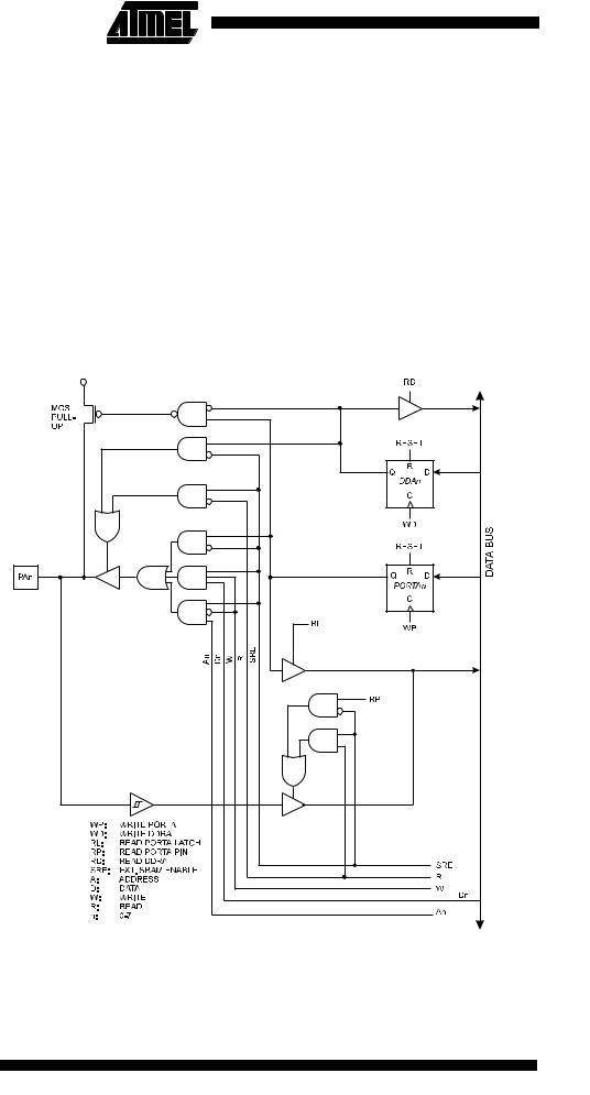
Port A Schematics |
Note that all port pins are synchronized. The synchronization latch is, however, not |
|
shown in the figure. |
|
Figure 56. Port A Schematic Diagrams (Pins PA0 - PA7) |
88 |
ATmega161(L) |
|
1228B–09/01 |

 ATmega161(L)
Port B
Port B Data Register – PORTB
Port B Data Direction Register
– DDRB
Port B Input Pins Address –
PINB
Port B is an 8-bit bi-directional I/O port.
Three I/O memory address locations are allocated for the Port B, one each for the Data Register – PORTB, $18($38), Data Direction Register – DDRB, $17($37) and the Port B Input Pins – PINB, $16($36). The Port B Input Pins address is read-only, while the Data Register and the Data Direction Register are read/write.
All port pins have individually selectable pull-up resistors. The Port B output buffers can sink 20 mA and thus drive LED displays directly. When pins PB0 to PB7 are used as inputs and are externally pulled low, they will source current if the internal pull-up resistors are activated.
The Port B pins with alternate functions are shown in Table 30.
Table 30. Port B Pin Alternate Functions(1)
Port Pin |
|
Alternate Functions |
|
|
|
|
|
PB0 |
|
OC0 (Timer/Counter0 Compare Match Output)/T0 (Timer/Counter0 External |
|
|
Counter Input) |
||
|
|
||
|
|
|
|
PB1 |
|
OC2 (Timer/Counter2 Compare Match Output)/T1 (Timer/Counter1 External |
|
|
Counter Input) |
||
|
|
||
|
|
|
|
PB2 |
|
RXD1 (UART1 Input Line)/AIN0 (Analog Comparator Positive Input) |
|
|
|
|
|
PB3 |
|
TXD1 (UART1 Output Line)/AIN1 (Analog Comparator Negative Input) |
|
|
|
|
|
PB4 |
|
|
(SPI Slave Select Input) |
SS |
|||
|
|
|
|
PB5 |
|
MOSI (SPI Bus Master Output/Slave Input) |
|
|
|
|
|
PB6 |
|
MISO (SPI Bus Master Input/Slave Output) |
|
|
|
|
|
PB7 |
|
SCK (SPI Bus Serial Clock) |
|
|
|
|
|
Note: 1. When the pins are used for the alternate function, the DDRB and PORTB registers have to be set according to the alternate function description.
Bit |
7 |
6 |
5 |
4 |
3 |
2 |
1 |
0 |
|
$18 ($38) |
PORTB7 |
PORTB6 |
PORTB5 |
PORTB4 |
PORTB3 |
PORTB2 |
PORTB1 |
PORTB0 |
PORTB |
|
|
|
|
|
|
|
|
|
|
Read/Write |
R/W |
R/W |
R/W |
R/W |
R/W |
R/W |
R/W |
R/W |
|
Initial Value |
0 |
0 |
0 |
0 |
0 |
0 |
0 |
0 |
|
Bit |
7 |
6 |
5 |
4 |
3 |
2 |
1 |
0 |
|
|
|
|
|
|
|
|
|
|
|
$17 ($37) |
DDB7 |
DDB6 |
DDB5 |
DDB4 |
DDB3 |
DDB2 |
DDB1 |
DDB0 |
DDRB |
|
|
|
|
|
|
|
|
|
|
Read/Write |
R/W |
R/W |
R/W |
R/W |
R/W |
R/W |
R/W |
R/W |
|
Initial Value |
0 |
0 |
0 |
0 |
0 |
0 |
0 |
0 |
|
Bit |
7 |
6 |
5 |
4 |
3 |
2 |
1 |
0 |
|
|
|
|
|
|
|
|
|
|
|
$16 ($36) |
PINB7 |
PINB6 |
PINB5 |
PINB4 |
PINB3 |
PINB2 |
PINB1 |
PINB0 |
PINB |
|
|
|
|
|
|
|
|
|
|
Read/Write |
R |
R |
R |
R |
R |
R |
R |
R |
|
Initial Value |
N/A |
N/A |
N/A |
N/A |
N/A |
N/A |
N/A |
N/A |
|
The Port B Input Pins address (PINB) is not a register; this address enables access to the physical value on each Port B pin. When reading PORTB, the Port B Data Latch is read and when reading PINB, the logical values present on the pins are read.
89
1228B–09/01
Port B as General Digital I/O All eight pins in Port B have equal functionality when used as digital I/O pins.
PBn, general I/O pin: The DDBn bit in the DDRB register selects the direction of this pin. If DDBn is set (one), PBn is configured as an output pin. If DDBn is cleared (zero), PBn is configured as an input pin. If PORTBn is set (one) when the pin is configured as an input pin, the MOS pull-up resistor is activated. To switch the pull-up resistor off, the PORTBn has to be cleared (zero) or the pin has to be configured as an output pin. The Port B pins are tri-stated when a reset condition becomes active, even if the clock is not running.
Table 31. DDBn Effects on Port B Pins(1)
DDBn |
|
PORTBn |
I/O |
Pull-up |
Comment |
|
|
|
|
|
|
0 |
|
0 |
Input |
No |
Tri-state (high-Z) |
|
|
|
|
|
|
0 |
|
1 |
Input |
Yes |
PBn will source current if ext. pulled low. |
|
|
|
|
|
|
1 |
|
0 |
Output |
No |
Push-pull Zero Output |
|
|
|
|
|
|
1 |
|
1 |
Output |
No |
Push-pull One Output |
|
|
|
|
|
|
Note: |
1. n: 7,6…0, pin number |
|
|
||
Alternate Functions of Port B The alternate pin configuration is as follows:
• SCK – Port B, Bit 7
SCK: Master clock output, slave clock input pin for SPI channel. When the SPI is enabled as a slave, this pin is configured as an input regardless of the setting of DDB7. When the SPI is enabled as a master, the data direction of this pin is controlled by DDB7. When the pin is forced to be an input, the pull-up can still be controlled by the PORTB7 bit. See the description of the SPI port for further details.
• MISO – Port B, Bit 6
MISO: Master data input, slave data output pin for SPI channel. When the SPI is enabled as a master, this pin is configured as an input regardless of the setting of DDB6. When the SPI is enabled as a slave, the data direction of this pin is controlled by DDB6. When the pin is forced to be an input, the pull-up can still be controlled by the PORTB6 bit. See the description of the SPI port for further details.
• MOSI – Port B, Bit 5
MOSI: SPI Master data output, slave data input for SPI channel. When the SPI is enabled as a slave, this pin is configured as an input regardless of the setting of DDB5. When the SPI is enabled as a master, the data direction of this pin is controlled by DDB5. When the pin is forced to be an input, the pull-up can still be controlled by the PORTB5 bit. See the description of the SPI port for further details.
• SS – Port B, Bit 4
SS: Slave port select input. When the SPI is enabled as a slave, this pin is configured as an input regardless of the setting of DDB5. As a slave, the SPI is activated when this pin is driven low. When the SPI is enabled as a master, the data direction of this pin is controlled by DDB5. When the pin is forced to be an input, the pull-up can still be controlled by the PORTB5 bit. See the description of the SPI port for further details.
• TXD1/AIN1 – Port B, Bit 3
AIN1, Analog Comparator Negative Input. This pin also serves as the negative input of the on-chip Analog Comparator.
TXD1, Transmit Data (Data output pin for the UART1). When the UART1 transmitter is enabled, this pin is configured as an output regardless of the value of DDRB3.
90 ATmega161(L)
1228B–09/01