Материал: DOC1228
ATmega161(L)
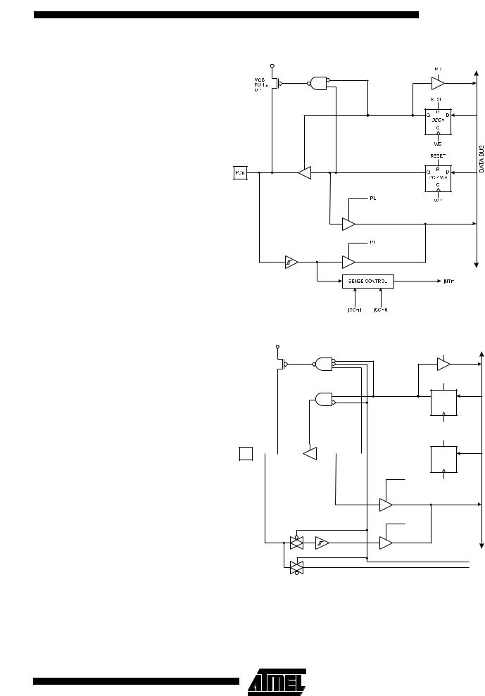
Figure 67. Port D Schematic Diagram (Pins PD2 and PD3)
WP: WRITE PORTD
WD: WRITE DDRD
RL: READ PORTD LATCH
RP: READ PORTD PIN
RD: READ DDRD
n:2, 3
m: |
0, 1 |
Figure 68. Port D Schematic Diagram (Pin PD4)
RD
MOS
PULL-
UP
RESET
R
Q D
DDD4
C
WD
RESET
R PD4 
 Q D
Q D
PORTD4
C
RL
WP
RP
DATA BUS
WP: |
WRITE PORTD |
WD: |
WRITE DDRD |
RL: |
READ PORTD LATCH |
RP: |
READ PORTD PIN |
RD: |
READ DDRD |
AS2: |
ASYNCH SELECT T/C2 |
AS2
T/C2 OSC AMP INPUT
101
1228B–09/01
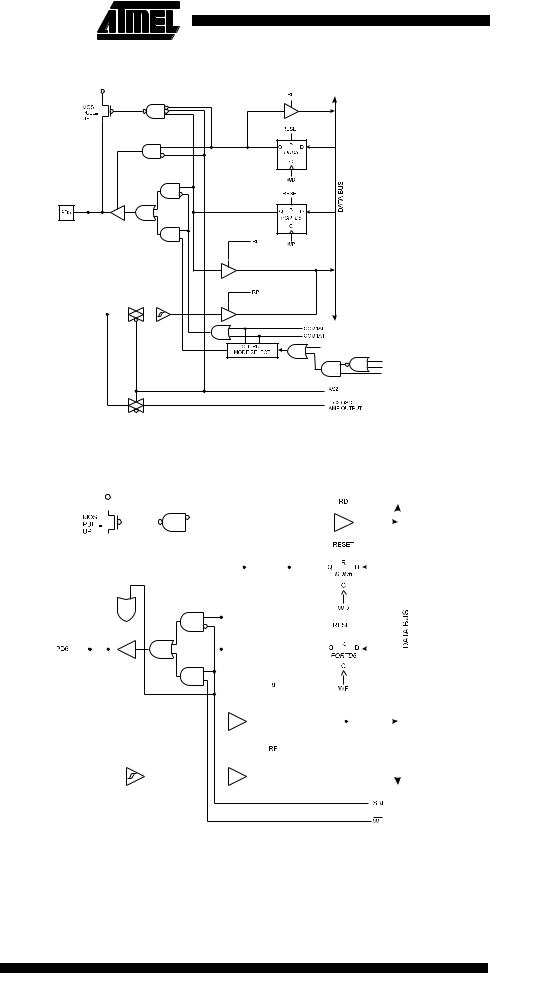
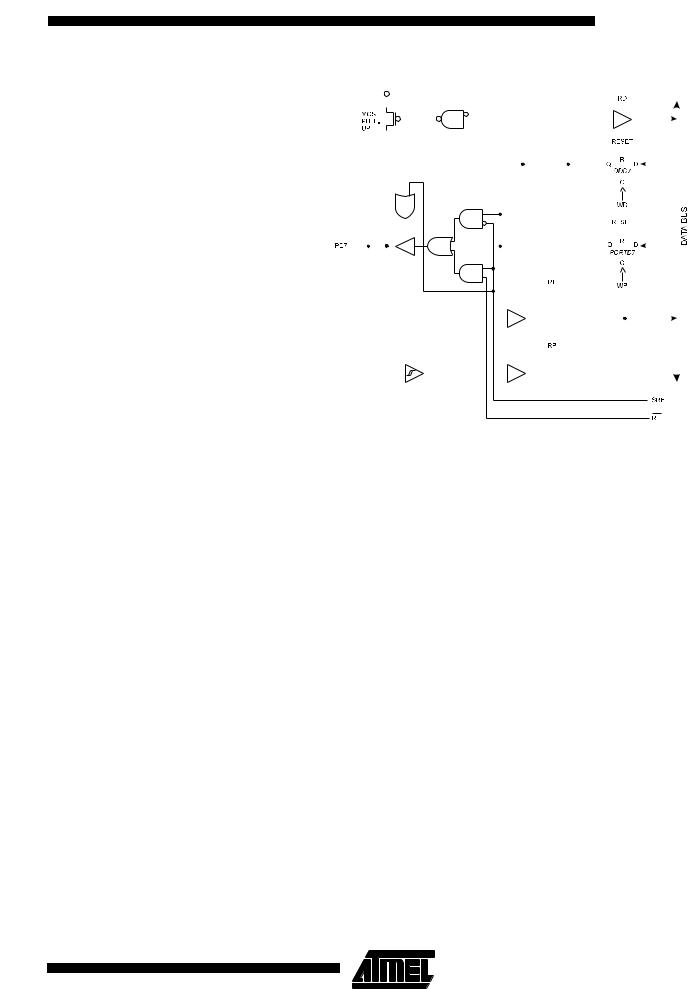
Figure 69. Port D Schematic Diagram (Pin PD5)
COMP. MATCH 1A
PWM10
PWM11
FOC1A
WP: |
WRITE PORTD |
WD: |
WRITE DDRD |
RL: |
READ PORTD LATCH |
RP: |
READ PORTD PIN |
RD: |
READ DDRD |
AS2 |
ASYNCH SELECT T/C2 |
Figure 70. Port D Schematic Diagram (Pin PD6)
|
|
|
|
|
|
|
|
|
|
|
|
|
|
|
|
|
|
|
|
|
|
|
|
|
|
|
|
|
|
|
|
|
|
|
|
|
|
|
|
|
|
|
|
|
|
|
|
|
|
|
|
|
|
|
|
|
|
|
|
|
|
|
|
|
|
|
|
|
|
|
|
|
|
|
|
|
|
|
|
|
|
|
|
|
|
|
|
|
|
|
|
|
|
|
|
|
|
|
|
|
|
|
|
|
|
|
|
|
|
|
|
|
|
|
|
|
|
|
|
|
|
|
|
|
|
|
|
|
|
|
|
|
|
|
|
|
|
|
|
|
|
|
|
|
|
|
|
|
|
|
|
|
|
|
|
|
|
|
|
|
|
|
|
|
|
|
|
|
|
|
|
|
|
|
|
|
|
|
|
|
|
|
|
|
|
|
|
|
|
|
|
|
|
|
|
|
|
|
|
|
|
|
|
|
|
|
|
|
|
|
|
|
|
|
|
|
|
|
|
|
|
|
|
|
|
|
|
|
|
|
|
|
|
|
|
|
|
|
|
|
|
|
|
|
|
|
|
|
|
|
|
|
|
|
|
|
|
|
|
|
|
|
|
|
|
|
|
|
|
|
|
|
|
|
|
|
|
|
|
|
|
|
|
|
|
|
|
|
|
|
|
|
|
|
|
|
|
|
|
|
|
|
|
|
|
|
|
|
|
|
|
|
|
|
|
|
|
|
|
|
|
|
|
|
|
|
|
|
|
|
|
|
|
|
|
|
|
|
|
|
|
|
|
|
|
|
|
|
|
|
|
|
|
|
|
|
|
|
|
|
|
|
|
|
|
|
|
|
|
|
|
|
|
|
|
|
|
|
|
|
|
|
|
|
|
|
|
|
|
|
|
|
|
|
|
|
|
|
|
|
|
|
|
|
|
|
|
|
|
|
|
|
|
|
|
|
|
|
|
|
|
|
|
|
|
|
|
|
|
|
|
|
|
|
|
|
|
|
|
|
|
|
|
|
|
|
|
|
|
|
|
|
|
|
|
|
|
|
|
|
|
|
|
|
|
|
|
|
|
|
|
|
|
|
|
|
|
|
|
|
|
|
|
|
|
|
|
|
|
|
|
|
|
|
|
|
|
|
|
|
|
|
|
|
|
|
|
|
|
|
|
|
|
|
|
|
|
|
|
|
|
|
|
|
|
|
|
|
|
|
|
|
|
|
|
|
|
|
|
|
|
|
|
|
|
|
|
|
|
|
|
|
|
|
|
|
|
|
|
|
|
|
|
|
|
|
|
|
|
|
|
|
|
|
|
|
|
|
|
|
|
|
|
|
|
|
|
|
|
WP: |
|
WRITE PORTD |
|
|
|
|
|
|
|
|
|
|
|
|
|||||||||||
|
|
|
|
|
|
|
|
|
|
|
|
|
|
|
|||||||||||||
|
|
WD: |
|
WRITE DDRD |
|
|
|
|
|
|
|
|
|
|
|
|
|||||||||||
|
|
RL: |
|
READ PORTD LATCH |
|
|
|
|
|
|
|
|
|
|
|
|
|||||||||||
|
|
RP: |
|
READ PORTD PIN |
|
|
|
|
|
|
|
|
|
|
|
|
|||||||||||
|
|
RD: |
|
READ DDRD |
|
|
|
|
|
|
|
|
|
|
|
|
|||||||||||
|
|
WE: |
|
WRITE ENABLE |
|
|
|
|
|
|
|
|
|
|
|
|
|
|
|
|
|||||||
|
SRE: |
|
EXTERNAL SRAM ENABLE |
|
|
|
|
|
|
|
|
|
|
|
|
||||||||||||
102 ATmega161(L)
1228B–09/01
ATmega161(L)
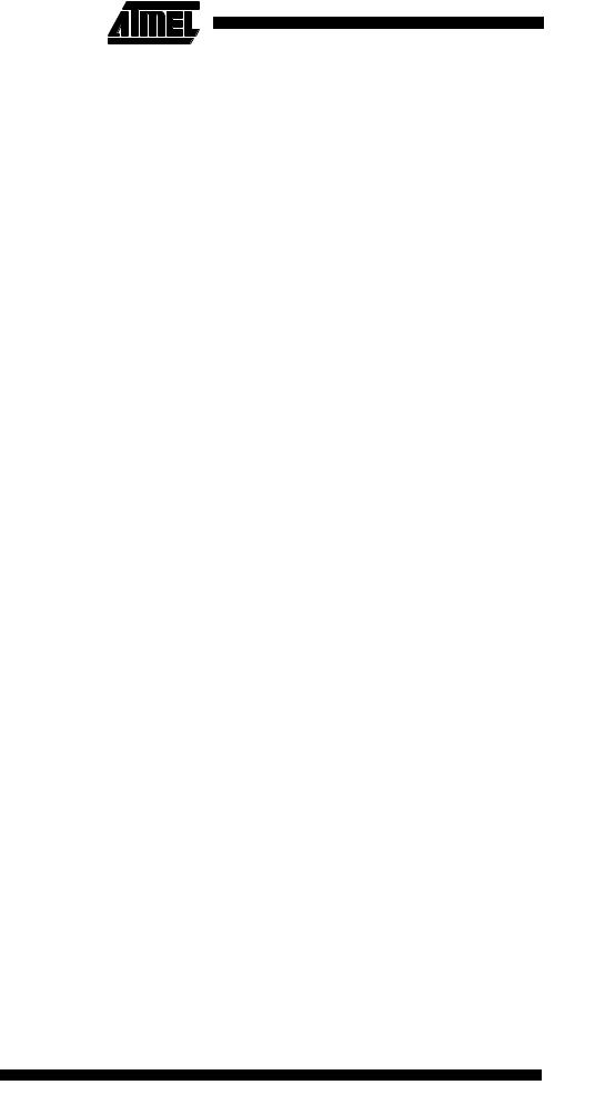
Figure 71. Port D Schematic Diagram (Pin PD7)
|
|
|
|
|
|
|
|
|
|
|
|
|
|
|
|
|
|
|
|
|
|
|
|
|
|
|
|
|
|
|
|
|
|
|
|
|
|
|
|
|
|
|
|
|
|
|
|
|
|
|
|
|
|
|
|
|
|
|
|
|
|
|
|
|
|
|
|
|
|
|
|
|
|
|
|
|
|
|
|
|
|
|
|
|
|
|
|
|
|
|
|
|
|
|
|
|
|
|
|
|
|
|
|
|
|
|
|
|
|
|
|
|
|
|
|
|
|
|
|
|
|
|
|
|
|
|
|
|
|
|
|
|
|
|
|
|
|
|
|
|
|
|
|
|
|
|
|
|
|
|
|
|
|
|
|
|
|
|
|
|
|
|
|
|
|
|
|
|
|
|
|
|
|
|
|
|
|
|
|
|
|
|
|
|
|
|
|
|
|
|
|
|
|
|
|
|
|
|
|
|
|
|
|
|
|
|
|
|
|
|
|
|
|
|
|
|
|
|
|
|
|
|
|
|
|
|
|
|
|
|
|
|
|
|
|
|
|
|
|
|
|
|
|
|
|
|
|
|
|
|
|
|
|
|
|
|
|
|
|
|
|
|
|
|
|
|
|
|
|
|
|
|
|
|
|
|
|
|
|
|
|
|
|
|
|
|
|
|
|
|
|
|
|
|
|
|
|
|
|
|
|
|
|
|
|
|
|
|
|
|
|
|
|
|
|
|
|
|
|
|
|
|
|
|
|
|
|
|
|
|
|
|
|
|
|
|
|
|
|
|
|
|
|
|
|
|
|
|
|
|
|
|
|
|
|
|
|
|
|
|
|
|
|
|
|
|
|
|
|
|
|
|
|
|
|
|
|
|
|
|
|
|
|
|
|
|
|
|
|
|
|
|
|
|
|
|
|
|
|
|
|
|
|
|
|
|
|
|
|
|
|
|
|
|
|
|
|
|
|
|
|
|
|
|
|
|
|
|
|
|
|
|
|
|
|
|
|
|
|
|
|
|
|
|
|
|
|
|
|
|
|
|
|
|
|
|
|
|
|
|
|
|
|
|
|
|
|
|
|
|
|
|
|
|
|
|
|
|
|
|
|
|
|
|
|
|
|
|
|
|
|
|
|
|
|
|
|
|
|
|
|
|
|
|
|
|
|
|
|
|
|
|
|
|
|
|
|
|
|
|
|
|
|
|
|
|
|
|
|
|
|
|
|
|
|
|
|
|
|
|
|
|
|
|
|
|
|
|
|
|
|
|
|
|
|
|
|
|
|
|
|
|
|
|
|
|
|
|
|
WP: |
|
WRITE PORTD |
|
|
|
|
|
|
|
|
|
|
|
|
|||||||||
|
|
|
|
|
|
|
|
|
|
|
|
|
|
|
|
|||||||||||
|
|
|
WD: |
|
WRITE DDRD |
|
|
|
|
|
|
|
|
|
|
|
|
|||||||||
|
|
|
RL: |
|
READ PORTD LATCH |
|
|
|
|
|
|
|
|
|
|
|
|
|||||||||
|
|
|
RP: |
|
READ PORTD PIN |
|
|
|
|
|
|
|
|
|
|
|
|
|||||||||
|
|
|
RD: |
|
READ DDRD |
|
|
|
|
|
|
|
|
|
|
|
|
|||||||||
|
|
|
RE: |
|
READ ENABLE |
|
|
|
|
|
|
|
|
|
|
|
|
|
|
|
||||||
|
|
SRE: |
|
EXTERNAL SRAM ENABLE |
|
|
|
|
|
|
|
|
|
|
|
|
||||||||||
103
1228B–09/01
Port E
Port E Data Register – PORTE
Port E Data Direction Register
– DDRE
Port E Input Pins Address –
PINE
Port E is a 3-bit bi-directional I/O port with internal pull-up resistors.
Three I/O address locations are allocated for the Port E, one each for the Data Register
– PORTE, $07($27), Data Direction Register – DDRE, $06($26) and the Port E Input Pins – PINE, $05($25). The Port E Input Pins address is read-only, while the Data Register and the Data Direction Register are read/write.
The Port E output buffers can sink 20 mA. As inputs, Port E pins that are externally pulled low will source current if the pull-up resistors are activated.
Port E pins have alternate functions as shown in Table 35.
Table 35. Port E Pin Alternate Functions(1)
Port Pin |
|
Alternate Function |
|
|
|
|
|
|
||
|
|
|
|
|
|
|
|
|
|
|
PE0 |
|
ICP (Input Capture Pin Timer/Counter1)/INT2 (External Interrupt 2 Input) |
|
|||||||
|
|
|
|
|
|
|
|
|
|
|
PE1 |
|
OC1B (Timer/Counter1 Output CompareB Match Output) |
|
|
||||||
|
|
|
|
|
|
|
|
|
|
|
PE2 |
|
ALE (Address Latch Enable, External Memory) |
|
|
|
|||||
|
|
|
|
|
|
|
|
|
|
|
Note: 1. |
When the PE1 pin is used for the alternate function, the DDRE and PORTE registers |
|||||||||
|
have to be set according to the alternate function description. |
|
|
|||||||
Bit |
7 |
6 |
5 |
4 |
3 |
2 |
1 |
0 |
|
|
$07 ($27) |
|
|
|
|
|
|
|
|
|
|
|
– |
– |
– |
– |
– |
PORTE2 |
PORTE1 |
PORTE0 |
PORTE |
|
|
|
|
|
|
|
|
|
|
|
|
Read/Write |
|
R |
R |
R |
R |
R |
R/W |
R/W |
R/W |
|
Initial Value |
0 |
0 |
0 |
0 |
0 |
0 |
0 |
0 |
|
|
Bit |
7 |
6 |
5 |
4 |
3 |
2 |
1 |
0 |
|
|
|
|
|
|
|
|
|
|
|
|
|
$06 ($26) |
|
– |
– |
– |
– |
– |
DDE2 |
DDE1 |
DDE0 |
DDRE |
|
|
|
|
|
|
|
|
|
|
|
Read/Write |
|
R |
R |
R |
R |
R |
R/W |
R/W |
R/W |
|
Initial Value |
0 |
0 |
0 |
0 |
0 |
0 |
0 |
0 |
|
|
Bit |
7 |
6 |
5 |
4 |
3 |
2 |
1 |
0 |
|
|
|
|
|
|
|
|
|
|
|
|
|
$05 ($25) |
|
– |
– |
– |
– |
– |
PINE2 |
PINE1 |
PINE0 |
PINE |
|
|
|
|
|
|
|
|
|
|
|
Read/Write |
|
R |
R |
R |
R |
R |
R |
R |
R |
|
Initial Value |
0 |
0 |
0 |
0 |
0 |
N/A |
N/A |
N/A |
|
|
The Port E Input Pins address (PINE) is not a register; this address enables access to the physical value on each Port E pin. When reading PORTE, the Port E Data Latch is read and when reading PINE, the logical values present on the pins are read.
Port E as General Digital I/O PEn, general I/O pin: The DDEn bit in the DDRE register selects the direction of this pin. If DDEn is set (one), PEn is configured as an output pin. If DDEn is cleared (zero), PEn is configured as an input pin. If PORTEn is set (one) when configured as an input pin, the MOS pull-up resistor is activated. To switch the pull-up resistor off, the PORTEn has to be cleared (zero) or the pin has to be configured as an output pin. The Port E pins are tri-stated when a reset condition becomes active, even if the clock is not running.
104 ATmega161(L)
1228B–09/01

|
|
|
|
|
|
|
ATmega161(L) |
|
|
|
|
|
|
|
|
|
|
Table 36. DDEn Bits on Port E Pins(1) |
|
||||
|
|
|
|
||||
|
|
|
|
||||
|
|
DDEn |
PORTEn |
I/O |
Pull-up |
Comment |
|
|
|
|
|
|
|
||
|
|
0 |
0 |
Input |
No |
Tri-state (high-Z) |
|
|
|
|
|
|
|
||
|
|
0 |
1 |
Input |
Yes |
PEn will source current if ext. pulled low. |
|
|
|
|
|
|
|
||
|
|
1 |
0 |
Output |
No |
Push-pull Zero Output |
|
|
|
|
|
|
|
||
|
|
1 |
1 |
Output |
No |
Push-pull One Output |
|
|
|
|
|
|
|
|
|
Note: 1. n: 2,1,0, pin number.
Alternate Functions of Port E The alternate pin configuration is as follows:
• OC1B – Port E, Bit 2
OC1B, Output compare match output: The PE2 pin can serve as an external output when the Timer/Counter1 compare matches. The PE2 pin has to be configured as an output (DDE2 set [one]) to serve this function. See “Timer/Counter1” on page 49 for further details. The OC1B pin is also the output pin for the PWM mode timer function.
• ALE – Port E, Bit 1
ALE: When the External Memory is enabled, the PE1 pin serves as the Dress Latch Enable. Note that enabling of External Memory will override both the direction and port value. See “Interface to External Memory” on page 82 for a detailed description.
• ICP/INT2 – Port E, Bit 0
ICP, input capture pin: The PE0 pin can serve as the input capture source for
Timer/Counter 1. See page 54 for a detailed description.
INT2, External Interrupt source 2: The PE0 pin can serve as an external interrupt source to the MCU. See “Extended MCU Control Register – EMCUCR” on page 36 for further details.
105
1228B–09/01