Материал: DOC1228
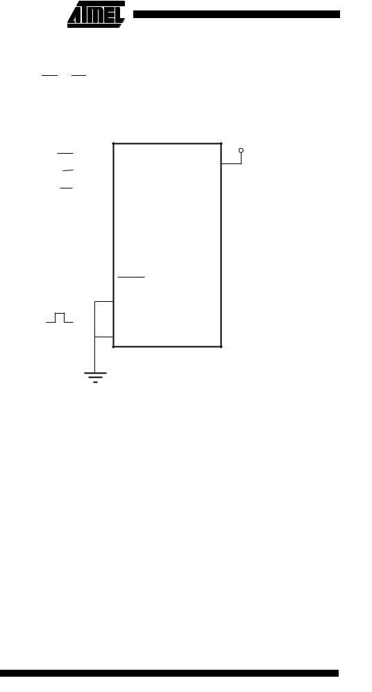
The XA1/XA0 pins determine the action executed when the XTAL1 pin is given a positive pulse. The bit codings are shown in Table 43.
When pulsing WR or OE, the command loaded determines the action executed. The command is a byte where the different bits are assigned functions as shown in Table 44.
Figure 76. Parallel Programming
ATmega161
+5V
RDY/BSY  PD1
PD1
VCC
OE  PD2
PD2
PB7 - PB0 
 DATA
DATA
WR  PD3
PD3
BS1  PD4
PD4
XA0  PD5
PD5
XA1  PD6
PD6
PAGEL  PD7
PD7
+12 V  RESET
RESET
PA0
 XTAL1
XTAL1
GND
Table 42. Pin Name Mapping
Signal Name in |
|
|
|
|
|
||||||
Programming Mode |
Pin Name |
I/O |
Function |
||||||||
|
|
|
|
|
|
|
|
|
|
|
|
|
|
|
|
|
|
|
PD1 |
O |
0: Device is busy programming; 1: Device is ready |
||
RDY/BSY |
|
||||||||||
|
|
|
|
|
|
|
|
|
for new command |
||
|
|
|
|
|
|
|
|
||||
|
|
|
|
|
|
PD2 |
I |
Output Enable (Active low) |
|||
OE |
|||||||||||
|
|
|
|
|
|
||||||
|
|
|
|
|
|
PD3 |
I |
Write Pulse (Active low) |
|||
WR |
|||||||||||
|
|
|
|
||||||||
BS1 |
PD4 |
I |
Byte Select 1 (“0” selects low byte, “1” selects |
||||||||
|
|
|
|
|
|
|
|
|
high byte) |
||
|
|
|
|
||||||||
XA0 |
PD5 |
I |
XTAL Action Bit 0 |
||||||||
|
|
|
|
||||||||
XA1 |
PD6 |
I |
XTAL Action Bit 1 |
||||||||
|
|
|
|
||||||||
PAGEL |
PD7 |
I |
Program Memory Page Load |
||||||||
|
|
|
|
||||||||
BS2 |
PA0 |
I |
Byte Select 2 (Always low) |
||||||||
|
|
|
|
|
|
||||||
DATA |
PB7 - 0 |
I/O |
Bi-directional Data Bus (Output when |
|
|
||||||
OE is low) |
|||||||||||
|
|
|
|
|
|
|
|
|
|
|
|
116 ATmega161(L)
1228B–09/01

|
|
|
|
|
ATmega161(L) |
|
|
|
|
|
|
|
|
|
|
|
|
|
|
Table 43. XA1 and XA0 Coding |
|||
|
|
||||
|
|
|
|
|
|
|
|
XA1 |
XA0 |
Action when XTAL1 is Pulsed |
|
|
|
|
|
||
|
|
0 |
0 |
Load Flash or EEPROM Address (High or low address byte determined by BS1) |
|
|
|
|
|
||
|
|
0 |
1 |
Load Data (High or low data byte for Flash determined by BS1) |
|
|
|
|
|
||
|
|
1 |
0 |
Load Command |
|
|
|
|
|
||
|
|
1 |
1 |
No Action, Idle |
|
|
|
|
|
|
|
Table 44. Command Byte Bit Coding
Command Byte |
Command Executed |
|
|
1000 0000 |
Chip Erase |
|
|
0100 0000 |
Write Fuse Bits |
|
|
0010 0000 |
Write Lock Bits |
|
|
0001 0000 |
Write Flash |
|
|
0001 0001 |
Write EEPROM |
|
|
0000 1000 |
Read Signature Bytes |
|
|
0000 0100 |
Read Fuse and Lock Bits |
|
|
0000 0010 |
Read Flash |
|
|
0000 0011 |
Read EEPROM |
|
|
Enter Programming Mode |
The following algorithm puts the device in parallel programming mode: |
|||||||||||
|
1. |
Apply 4.5 - 5.5V between VCC and GND. |
||||||||||
|
2. |
Set |
|
|
|
and BS pins to “0” and wait at least 500 ns. |
||||||
|
RESET |
|||||||||||
|
3. |
Apply 11.5 - 12.5V to |
|
and wait for at least 500 ns. |
||||||||
|
RESET, |
|||||||||||
Chip Erase |
The Chip Erase will erase the Flash and EEPROM memories plus Lock bits. The Lock |
|||||||||||
|
bits are not reset until the program memory has been completely erased. The Fuse bits |
|||||||||||
|
are not changed. A Chip Erase must be performed before the Flash is reprogrammed. |
|||||||||||
|
Load Command “Chip Erase” |
|||||||||||
|
1. |
Set XA1, XA0 to “10”. This enables command loading. |
||||||||||
|
2. |
Set BS1 to “0”. |
||||||||||
|
3. |
Set DATA to “1000 0000”. This is the command for Chip Erase. |
||||||||||
|
4. |
Give |
|
|
|
|
|
goes low. |
||||
|
WR |
a negative pulse. This starts the Chip Erase. RDY/BSY |
||||||||||
|
5. |
|
|
goes high before loading a new command. |
||||||||
|
Wait until RDY/BSY |
|||||||||||
Programming the Flash |
The Flash is organized as 128 pages of 128 bytes each. When programming the Flash, |
|||||||||||
|
the program data is latched into a page buffer. This allows one page of program data to |
|||||||||||
|
be programmed simultaneously. The following procedure describes how to program the |
|||||||||||
|
entire Flash memory: |
|||||||||||
A. Load Command “Write Flash”
1.Set XA1, XA0 to “10”. This enables command loading.
2.Set BS1 to “0”.
3.Set DATA to “0001 0000”. This is the command for Write Flash.
4.Give XTAL1 a positive pulse. This loads the command.
117
1228B–09/01
B. Load Address Low Byte
1.Set XA1, XA0 to “00”. This enables address loading.
2.Set BS1 to “0”. This selects low address.
3.Set DATA = Address low byte ($00 - $FF).
4.Give XTAL1 a positive pulse. This loads the address low byte.
C. Load Data Low Byte
1.Set BS1 to “0”. This selects low data byte.
2.Set XA1, XA0 to “01”. This enables data loading.
3.Set DATA = Data low byte ($00 - $FF).
4.Give XTAL1 a positive pulse. This loads the data byte.
D. Latch Data Low Byte
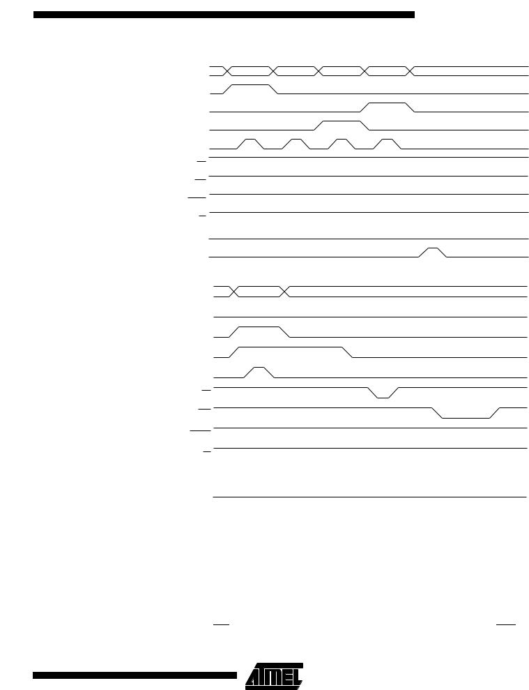
Give PAGEL a positive pulse. This latches the data low byte. (See Figure 77 for signal waveforms.)
E. Load Data High Byte
1.Set BS1 to “1”. This selects high data byte.
2.Set XA1, XA0 to “01”. This enables data loading.
3.Set DATA = Data high byte ($00 - $FF).
4.Give XTAL1 a positive pulse. This loads the data byte.
F. Latch Data High Byte
Give PAGEL a positive pulse. This latches the data high byte.
G. Repeat “B” through “F” 64 times to fill the page buffer.
To address a page in the Flash, seven bits are needed (128 pages). The five most significant bits are read from address high byte as described in section “H” below. The two least significant page address bits, however, are the two most significant bits (bit7 and bit6) of the latest loaded address low byte as described in section “B”.
H. Load Address High byte
1.Set XA1, XA0 to “00”. This enables address loading.
2.Set BS1 to “1”. This selects high address.
3.Set DATA = Address high byte ($00 - $1F).
4.Give XTAL1 a positive pulse. This loads the address high byte.
I. Program Page
1.Give WR a negative pulse. This starts programming of the entire page of data. RDY/BSYgoes low.
2.Wait until RDY/BSY goes high.
(See Figure 78 for signal waveforms.)
J. End Page Programming
1.Set XA1, XA0 to “10”. This enables command loading.
2.Set DATA to “0000 0000”. This is the command for No Operation.
3.Give XTAL1 a positive pulse. This loads the command, and the internal write signals are reset.
K. Repeat “A” through “J” 128 times or until all data have been programmed.
118 ATmega161(L)
1228B–09/01
ATmega161(L)
Figure 77. Programming the Flash Waveforms
DATA |
$10 |
ADDR. LOW |
ADDR. HIGH |
DATA LOW |
XA1
XA2
BS1
XTAL1
WR
RDY/BSY
RESET +12V
OE
BS2
PAGEL
Figure 78. Programming the Flash Waveforms (Continued)
DATA |
DATA HIGH |
XA1
XA0
BS1
XTAL1
WR
RDY/BSY
RESET +12V
OE
PAGEL 
BS2
Programming the EEPROM The programming algorithm for the EEPROM data memory is as follows (refer to “Programming the Flash” for details on command, address and data loading):
1.A: Load Command “0001 0001”.
2.H: Load Address High Byte ($00 - $01)
3.B: Load Address Low Byte ($00 - $FF)
4.E: Load Data Low Byte ($00 - $FF)
L: Write Data Low Byte
1.Set BS to “0”. This selects low data.
2.Give WR a negative pulse. This starts programming of the data byte. RDY/BSY goes low.
119
1228B–09/01
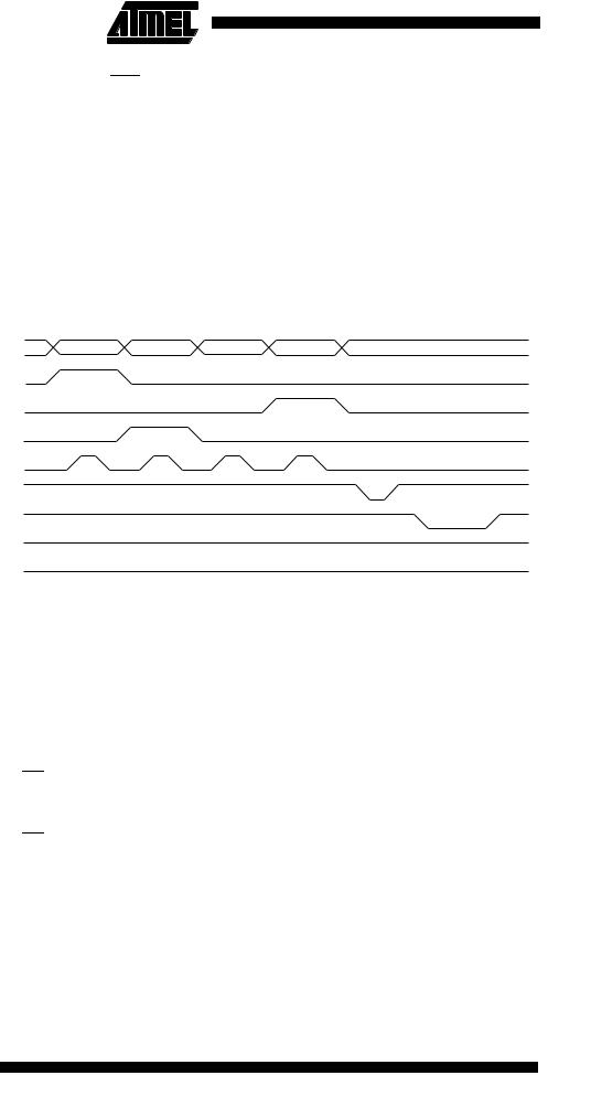
3.Wait until to RDY/BSY goes high before programming the next byte. (See Figure 79 for signal waveforms.)
The loaded command and address are retained in the device during programming. For efficient programming, the following should be considered:
•The command needs to be loaded only once when writing or reading multiple memory locations.
•Address high byte only needs to be loaded before programming a new 256-word page in the EEPROM.
•Skip writing the data value $FF, that is, the contents of the entire EEPROM after a Chip Erase.
These considerations also apply to Flash, EEPROM and Signature bytes reading.
Figure 79. Programming the EEPROM Waveforms
|
|
DATA |
$11 |
ADDR. HIGH ADDR. LOW |
DATA LOW |
|||||
|
|
|
XA1 |
|
|
|
|
|
||
|
|
|
XA2 |
|
|
|
|
|
||
|
|
|
BS1 |
|
|
|
|
|
||
|
|
XTAL1 |
|
|
|
|
|
|||
|
|
|
|
|
|
|
|
|
|
|
|
|
|
|
WR |
|
|
|
|
|
|
|
|
|
|
|
|
|
|
|
|
|
|
RDY/BSY |
|
|
|
|
|
||||
|
|
|
|
|
|
+12V |
|
|
|
|
|
|
RESET |
|
|
|
|||||
|
|
|
|
|
|
|
|
|
|
|
|
|
|
|
OE |
|
|
|
|
|
|
|
|
|
BS2 |
|
|
|
|
|
||
Reading the Flash |
|
PAGEL |
|
|
|
|
|
|||
The algorithm for reading the Flash memory is as follows (refer to “Programming the |
||||||||||
|
Flash” on page 117 for details on command and address loading): |
|||||||||
1.A: Load Command “0000 0010”.
2.H: Load Address High Byte ($00 - $1F)
3.B: Load Address Low Byte ($00 - $FF)
4.Set OE to “0”, and BS1 to “0”. The Flash word low byte can now be read at DATA.
5.Set BS to “1”. The Flash word high byte can now be read at DATA.
6.Set OE to “1”.
Reading the EEPROM |
The algorithm for reading the EEPROM memory is as follows (refer to “Programming the |
||||
|
Flash” on page 117 for details on command and address loading): |
||||
|
1. |
A: Load Command “0000 0011”. |
|||
|
2. |
H: Load Address High Byte ($00 - $01) |
|||
|
3. |
B: Load Address ($00 - $FF) |
|||
|
4. |
Set |
|
|
to “0”, and BS1 to “0”. The EEPROM Data byte can now be read at |
|
OE |
||||
|
|
DATA. |
|||
|
5. |
Set |
|
to “1”. |
|
|
OE |
||||
120 ATmega161(L)
1228B–09/01