Материал: DOC1228

ATmega161(L)
Programming the Fuse Bits The algorithm for programming the Fuse bits is as follows (refer to “Programming the Flash” on page 117 for details on command and data loading):
1.A: Load Command “0100 0000”.
2.C: Load Data Low Byte. Bit n = “0” programs and bit n = “1” erases the Fuse bit. Bit 6 = BOOTRST Fuse bit
Bit 5 = SPIEN Fuse bit
Bit 4 = BODLEVEL Fuse bit Bit 3 = BODEN Fuse bit
Bits 2 - 0 = CKSEL2..0 Fuse bits
Bit 7 = “1”. This bit is reserved and should be left unprogrammed (“1”).
3.Give WR a negative pulse and wait for RDY/BSY to go high.
Programming the Lock Bits The algorithm for programming the Lock bits is as follows (refer to “Programming the Flash” on page 117 for details on command and data loading):
1.A: Load Command “0010 0000”.
2.D: Load Data Low Byte. Bit n = “0” programs the Lock bit. Bit 5 = Boot Lock Bit12
Bit 4 = Boot Lock Bit11 Bit 3 = Boot Lock Bit02 Bit 2 = Boot Lock Bit01 Bit 1 = Lock Bit2
Bit 0 = Lock Bit1
Bits 7 - 6 = “1”. These bits are reserved and should be left unprogrammed (“1”).
3.L: Write Data Low Byte.
The Lock bits can only be cleared by executing Chip Erase.
Reading the Fuse and Lock |
The algorithm for reading the Fuse and Lock bits is as follows (refer to “Programming |
|||||||
Bits |
the Flash” on page 117 for details on command loading): |
|||||||
|
1. |
A: Load Command “0000 0100”. |
||||||
|
2. |
Set |
|
|
|
|
to “0”, and BS to “0”. The status of the Fuse bits can now be read at |
|
|
OE |
|||||||
|
|
DATA (“0” means programmed). |
||||||
|
|
Bit 6 = BOOTRST Fuse bit |
||||||
|
|
Bit 5 = SPIEN Fuse bit |
||||||
|
|
Bit 4 = BODLEVEL Fuse bit |
||||||
|
|
Bit 3 = BODEN Fuse bit |
||||||
|
|
Bits 2 - 0 = CKSEL2..0 Fuse bits |
||||||
|
3. |
Set |
|
|
to “0”, and BS to “1”. The status of the Lock bits can now be read at |
|||
|
OE |
|||||||
|
|
DATA (“0” means programmed). |
||||||
|
|
Bit 5 = Boot Lock Bit12 |
||||||
|
|
Bit 4 = Boot Lock Bit11 |
||||||
|
|
Bit 3 |
= Boot Lock Bit02 |
|||||
|
|
Bit 2 |
= Boot Lock Bit01 |
|||||
|
|
Bit 1 |
= Lock Bit2 |
|||||
|
|
Bit 0 |
= Lock Bit1 |
|||||
|
4. |
Set |
|
to “1”. |
||||
|
OE |
|||||||
Reading the Signature Bytes The algorithm for reading the Signature bytes is as follows (refer to “Programming the Flash” on page 117 for details on command and address loading):
1.A: Load Command “0000 1000”.
2.C: Load Address Low Byte ($00 - $02).
121
1228B–09/01
Parallel Programming
Characteristics
Set OE to “0”, and BS to “0”. The selected Signature byte can now be read at DATA. 3. Set OE to “1”.
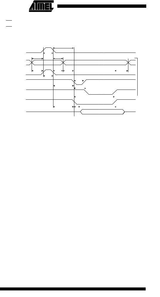
Figure 80. Parallel Programming Timing
tXLWL
XTAL1 |
tXHXL |
tDVXH tXLDX
Data & Control (DATA, XA0/1, BS1)
PAGEL |
tBVXH |
|
|
|
tPLBX tBVWL |
|
|
|
|
|
|
|
|
|
|
|
tRHBX |
|
|
|||||||||
|
|
tPHPL |
|
|
|
|
|
|
|
|
|
|
|
|
|
|
|
|
|
|
||||||||
|
|
|
|
|
|
|
|
|
|
|
|
tWLWH |
|
|
|
|
|
|
|
|
|
|
|
Write |
||||
|
|
|
|
|
|
|
|
|
|
|
|
|
|
|
|
|
|
|
||||||||||
|
WR |
|
|
tPLWL |
|
|
|
|
|
|
|
|
|
|
|
|
|
|
|
|
||||||||
|
|
|
|
|
|
|
|
|
|
WLRL |
|
|
|
|
|
|
|
|
|
|||||||||
|
|
|
|
|
|
|
|
|
|
|
|
|
|
|
|
|
|
|
|
|
|
|||||||
|
|
|
|
|
|
|
|
|
|
|
|
|
|
|
|
|
|
|
|
|
|
|
|
|
|
|
|
|
RDY/BSY |
|
|
|
|
|
|
|
|
|
|
|
|
|
|
|
|
|
|
|
|
|
|
||||||
|
|
|
|
|
|
|
|
|
|
|
|
|
|
|
|
|
|
|
|
|
|
|
tWLRH |
|
|
|||
|
|
|
|
|
|
|
|
|
|
|
|
|
|
|
|
|
|
|
|
|
|
|
|
|||||
|
|
|
|
|
|
|
|
|
|
|
|
|
|
|
|
|
|
|
|
|
|
|
|
|||||
|
|
|
|
|
|
|
|
|
|
|
|
|
|
|
|
|
|
|
|
|
|
|
|
|
|
|
|
|
|
OE |
|
|
tXLOL |
|
|
|
|
|
|
|
|
|
|
|
tOHDZ |
|
|
|
Read |
||||||||
DATA |
|
|
|
|
|
tOLDV |
|
|
|
|
||||||||||||||||||
|
|
|
|
|
|
|
|
|
|
|
|
|
|
|
||||||||||||||
|
|
|
|
|
|
|
|
|
|
|
|
|
|
|
|
|
|
|
|
|
|
|||||||
|
|
|
|
|
|
|
|
|
|
|
|
|
|
|
|
|
|
|
|
|
|
|
|
|
|
|
|
|
122 ATmega161(L)
1228B–09/01

 ATmega161(L)
Serial Downloading
Table 45. |
Parallel Programming Characteristics, TA = 25°C ± 10%, VCC = 5V ± |
||||||||||||||||||||
10%(1)(2)(3) |
|
|
|
|
|
|
|
|
|
|
|
|
|
|
|
|
|
|
|
|
|
Symbol |
|
|
|
|
|
|
|
|
|
|
|
Parameter |
Min |
Typ |
Max |
Units |
|||||
|
|
|
|
|
|
|
|
||||||||||||||
VPP |
|
|
Programming Enable Voltage |
11.5 |
|
12.5 |
V |
||||||||||||||
IPP |
|
|
Programming Enable Current |
|
|
250 |
µA |
||||||||||||||
tDVXH |
|
|
Data and Control Valid before XTAL1 High |
67 |
|
|
ns |
||||||||||||||
tXHXL |
|
|
XTAL1 Pulse Width High |
67 |
|
|
ns |
||||||||||||||
tXLDX |
|
|
Data and Control Hold after XTAL1 Low |
67 |
|
|
ns |
||||||||||||||
tXLWL |
|
|
XTAL1 Low to |
|
|
|
|
|
|
Low |
67 |
|
|
ns |
|||||||
WR |
|
||||||||||||||||||||
tBVXH |
|
|
BS1 Valid before XTAL1 High |
67 |
|
|
ns |
||||||||||||||
tPHPL |
|
|
PAGEL Pulse Width High |
67 |
|
|
ns |
||||||||||||||
tPLBX |
|
|
BS1 Hold after PAGEL Low |
67 |
|
|
ns |
||||||||||||||
tPLWL |
|
|
PAGEL Low to |
|
|
|
|
|
Low |
67 |
|
|
ns |
||||||||
WR |
|
||||||||||||||||||||
tBVWL |
|
|
BS1 Valid to |
|
|
|
|
Low |
67 |
|
|
ns |
|||||||||
WR |
|
||||||||||||||||||||
tRHBX |
|
|
|
|
|
|
|
|
|
|
|
|
|
|
|
|
|
|
|
|
|
|
|
BS1 Hold after RDY/BSY |
High |
67 |
|
|
ns |
||||||||||||||
tWLWH |
|
|
|
|
|
Pulse Width Low |
67 |
|
|
ns |
|||||||||||
|
|
WR |
|
||||||||||||||||||
tWLRL |
|
|
|
|
|
|
|
|
|
|
|
|
|
|
|
Low |
0 |
|
2.5 |
µs |
|
|
|
WR |
Low to RDY/BSY |
||||||||||||||||||
tWLRH |
|
|
|
|
|
|
|
|
|
|
|
|
|
|
|
High(1) |
1 |
|
1.7 |
ms |
|
|
|
WR |
Low to RDY/BSY |
||||||||||||||||||
tWLRH_CE |
|
|
|
|
|
|
|
|
|
|
|
|
|
|
|
High for Chip Erase(2) |
16 |
|
28 |
ms |
|
|
|
WR |
Low to RDY/BSY |
||||||||||||||||||
tWLRH_FLASH |
|
|
|
|
|
|
|
|
|
|
|
|
|
|
|
High for Write Flash(3) |
8 |
|
14 |
ms |
|
|
|
WR |
Low to RDY/BSY |
||||||||||||||||||
tXLOL |
|
|
XTAL1 Low to |
|
|
|
|
Low |
67 |
|
|
ns |
|||||||||
|
|
OE |
|
||||||||||||||||||
tOLDV |
|
|
|
|
Low to DATA Valid |
|
20 |
|
ns |
||||||||||||
|
|
OE |
|
||||||||||||||||||
tOHDZ |
|
|
|
|
High to DATA Tri-stated |
|
|
20 |
ns |
||||||||||||
|
|
OE |
|
|
|||||||||||||||||
Notes: 1. tWLRH is valid for the Write EEPROM, Write Fuse Bits and Write Lock Bits commands.
2.tWLRH_CE is valid for the Chip Erase command.
3.tWLRH_FLASH is valid for the Write Flash command.
Both the Flash and EEPROM memory arrays can be programmed using the serial SPI bus while RESET is pulled to GND. The serial interface consists of pins SCK, MOSI (input) and MISO (output). After RESET is set low, the Programming Enable instruction needs to be executed first, before program/erase operations can be executed.
When programming the EEPROM, an auto-erase cycle is built into the self-timed programming operation (in the serial mode ONLY) and there is no need to first execute the Chip Erase instruction. The chip erase operation turns the contents of every memory location in both the program and EEPROM arrays into $FF.
The program and EEPROM memory arrays have separate address spaces:
$0000 to $1FFF for program memory and $0000 to $01FF for EEPROM memory.
Either an external system clock is supplied at pin XTAL1 or a crystal needs to be connected across pins XTAL1 and XTAL2. The minimum low and high periods for the serial clock (SCK) input are defined as follows:
Low: > 2 XTAL1 clock cycles
High: > 2 XTAL1 clock cycles
123
1228B–09/01
Serial Programming
Algorithm
Data Polling Flash
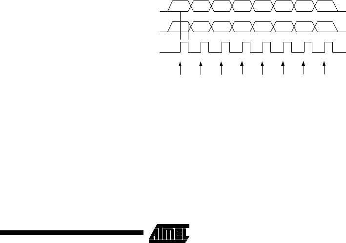
When writing serial data to the ATmega161, data is clocked on the rising edge of SCK.
When reading data from the ATmega161, data is clocked on the falling edge of SCK. See Figure 81, Figure 82 and Table 49 for timing details.
To program and verify the ATmega161 in the serial programming mode, the following sequence is recommended (see 4-byte instruction formats in Table 48):
1.Power-up sequence:
Apply power between VCC and GND while RESET and SCK are set to “0”. If a crystal is not connected across pins XTAL1 and XTAL2, apply a clock signal to the XTAL1 pin. In some systems, the programmer cannot guarantee that SCK is held low during power-up. In this case, RESET must be given a positive pulse of at least two XTAL1 cycles’ duration after SCK has been set to “0”.
2.Wait for at least 20 ms and enable serial programming by sending the Programming Enable serial instruction to pin MOSI/PB5.
3.The serial programming instructions will not work if the communication is out of synchronization. When in sync, the second byte ($53) will echo back when issuing the third byte of the Programming Enable instruction. Whether or not the echo is correct, all four bytes of the instruction must be transmitted. If the $53 did not echo back, give RESET a positive pulse and issue a new Programming Enable command.
4.If a chip erase is performed (must be done to erase the Flash), give RESET a positive pulse and start over from step 2.
5.The Flash is programmed one page at a time. The memory page is loaded one byte at a time by supplying the 6 LSB of the address and data together with the Load Program Memory Page instruction. The Program Memory Page is stored by loading the Write Program Memory Page instruction with the 7 MSB of the
address. If polling is not used, the user must wait at least tWD_FLASH before issuing the next page (please refer to Table 46). Accessing the serial programming interface before the Flash write operation completes can result in incorrect programming.
6.The EEPROM array is programmed one byte at a time by supplying the address and data together with the appropriate Write instruction. An EEPROM memory location is first automatically erased before new data is written. If polling is not
used, the user must wait at least tWD_EEPROM before issuing the next byte (please refer to Table 46). In a chip-erased device, no $FFs in the data file(s) need to be programmed.
7.Any memory location can be verified by using the Read instruction, which returns the content at the selected address at serial output MISO/PB6.
8.At the end of the programming session, RESET can be set high to commence normal operation.
9.Power-off sequence (if needed):
Set XTAL1 to “0” (if a crystal is not used). Set RESET to “1”.
Turn VCC power off.
When a page is being programmed into the Flash, reading an address location within the page being programmed will give the value $FF. At the time the device is ready for a new page, the programmed value will read correctly. This is used to determine when the next page can be written. Note that the entire page is written simultaneously and any address within the page can be used for polling. Data polling of the FLASH will not work for the value $FF, so when programming this value, the user will have to wait for at least
124 ATmega161(L)
1228B–09/01
|
|
|
|
|
|
ATmega161(L) |
|
|
|
|
|
|
|
|
|
|
|
|
|
|
|
|
tWD_FLASH before programming the next page. As a chip-erased device contains $FF in |
||||
|
|
|||||
|
|
all locations, programming of addresses that are meant to contain $FF can be skipped. |
||||
|
|
See Table 46 for tWD_FLASH value. |
|
|
||
Data Polling EEPROM |
When a new byte has been written and is being programmed into EEPROM, reading the |
|||||
|
|
address location being programmed will give the value $FF. At the time the device is |
||||
|
|
ready for a new byte, the programmed value will read correctly. This is used to deter- |
||||
|
|
mine when the next byte can be written. This will not work for the value $FF, but the user |
||||
|
|
should keep the following in mind: As a chip-erased device contains $FF in all locations, |
||||
|
|
programming of addresses that are meant to contain $FF can be skipped. This does not |
||||
|
|
apply if the EEPROM is reprogrammed without chip-erasing the device. In this case, |
||||
|
|
data polling cannot be used for the value $FF, and the user will have to wait at least |
||||
|
|
tWD_EEPROM before programming the next byte. See Table 46 for tWD_EEPROM value. |
||||
|
|
Table 46. Minimum Wait Delay before Writing the Next Flash or EEPROM Location |
||||
|
|
|
|
|
|
|
|
|
Symbol |
|
Minimum Wait Delay |
||
|
|
|
|
|
|
|
|
|
tWD_FLASH |
|
14 ms |
||
|
|
tWD_EEPROM |
|
3.4 ms |
||
|
|
Table 47. Minimum Wait Delay after a Chip Erase Command |
||||
|
|
|
|
|
||
|
|
Symbol |
|
|
Minimum Wait Delay |
|
|
|
|
|
|
||
|
|
tWD_ERASE |
|
|
28 ms |
|
Figure 81. Serial Programming Waveforms
SERIAL DATA INPUT |
MSB |
LSB |
PB5 (MOSI) |
|
|
SERIAL DATA OUTPUT |
MSB |
LSB |
PB6 (MISO) |
|
|
SERIAL CLOCK INPUT |
|
|
PB7(SCK) |
|
|
SAMPLE |
|
|
125
1228B–09/01