Материал: m013800e
Structure of CONTROL and STATUS byte
CONTROL Byte
|
E |
|
E |
E |
E |
E |
E |
E |
E |
|
5(*B5(4 |
|
|
|
79' 5(4 |
6(7B4 |
6(7B4 |
5$1*(B6(/ |
5$1*(B6(/ |
|
|
|
|
|
|
|
|
5(4 |
5(4 |
|
5(*B5(4 |
|
15' :5 |
5(*B$ |
5(*B$ |
5(*B$ |
5(*B$ |
5(*B$ |
5(*B$ |
|
Bit |
|
|
Description |
|
|
|
|
|
||
|
|
|
|
|
|
|
|
|
|
|
|
|
|
|
|
|
|
|
|
|
|
|
|
|
5(*B5(4 |
|
|
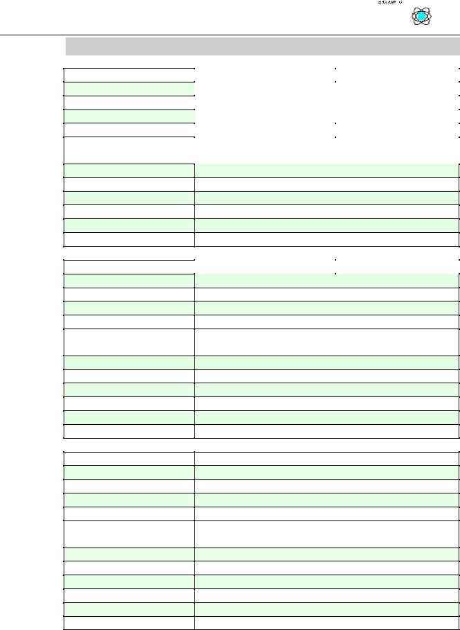
$FFHVV WR WKH UHJLVWHU VWUXFWXUH LV UHTXHVWHG E E FRQWDLQ WKH DGGUHVV RI WKH UHJLVWHU |
|
||||||
|
5(*B$ $ |
5HJLVWHU DGGUHVV |
|
|
|
|
|
||||
|
79' 5(4 |
|
|
5HTXHVW WR FKDQJH WKH PD[LPXP WLPH ZLWKRXW YDOLG GDWD |
|
|
|
||||
|
|
|
|
|
|
||||||
|
6(7B4 |
|
|
&RQWURO 2XWSXW 4 4 RII 4 RQ |
|
|
|
|
|||
|
6(7B4 |
|
|
&RQWURO 2XWSXW 4 4 RII 4 RQ |
|
|
|
|
|||
|
|
|
|
|
|
|
|||||
|
5$1*(B6(/ 5(4 |
6HOHFWLRQ RI WKH LQWHJUDWLRQ WLPH DQG WKH UHSUHVHQWDWLRQ RI PHDVXUHG IUHTXHQF\ YDOXH |
|
||||||||
|
5$1*(B6(/ 5(4 |
6HOHFWLRQ RI WKH LQWHJUDWLRQ WLPH DQG WKH UHSUHVHQWDWLRQ RI PHDVXUHG IUHTXHQF\ YDOXH |
|
||||||||
|
STATUS Byte |
|
|
|
|
|
|
||||
|
E |
|
|
|
E |
E |
E |
E |
E |
E |
E |
|
5(*B$&. |
|
|
|
|
67B*$7( |
79' $&. |
67B4 |
67B4 |
5$1*(B6(/ |
5$1*(B6(/ |
|
|
|
|
|
|
|
|
|
|
$&. |
$&. |
|
5(*B$&. |
|
|
|
|
5(*B$ |
5(*B$ |
5(*B$ |
5(*B$ |
5(*B$ |
5(*B$ |
Bit |
Description |
|
|
|
|
5(*B$&. |
$FNQRZOHGJPHQW WR WKH UHJLVWHU UHTXHVW E E FRQWDLQ WKH DGGUHVV RI WKH UHJLVWHU |
|
5(*B$ $ |
5HJLVWHU DGGUHVV |
|
67B*$7( |
6WDWH RI *$7( LQSXW HQDEOHG GLVDEOHG |
|
79' $&. |
$FNQRZOHGJPHQW 79' FKDQJHG |
|
67B$ |
6WDWH RI RXWSXW 4 |
|
67B$ |
6WDWH RI RXWSXW 4 |
|
5$1*(B6(/ $&. |
$FNQRZOHGJPHQW WR 5DQJH 6HOHFWLRQ )UHTXHQF\ YDOXHV DUH YDOLG |
|
5$1*(B6(/ $&. |
$FNQRZOHGJPHQW WR 5DQJH 6HOHFWLRQ )UHTXHQF\ YDOXHV DUH YDOLG |
Counter 750-404 |
11 |
:$*2Ç, 2Ç6<67(0
Structure of Input and Output data
The input data contain the CLOCK frequency as a binary value. The representation depends on the RANGE_SEL bits in the CONTROL byte. Even the method of measuring is selected via these bits. The following table illustrates the different modes.
5$1*(B6(/
5$1*(B6(/ 0HWKRG RI PHDVXUHPHQW
,QWHJUDWLRQ RYHU SHULRG
,QWHJUDWLRQ RYHU SHULRGV
,QWHJUDWLRQ RYHU SHULRGV
,QWHJUDWLRQ RYHU SHULRGV
5HSUHVHQWDWLRQ RI PHDVXULQJ YDOXH
)UHTXHQF\ LQ +] )UHTXHQF\ LQ +] )UHTXHQF\ LQ +] )UHTXHQF\ LQ +]
Attention:
When a new frequency range is requested, the application has to wait for valid data until the RANGE_SEL ACK bits contain the new frequency range. The maximum delay can be calculated using the following formula
TDmax= 2 * |
number of periods to be integrated |
actual frequency |
If the gate is enabled the input data contains the last valid frequency value. In this state the application cannot request a new range.
The valid frequency range stretches from 0.1 Hz up to 10 kHz (100000D).
To recognize static CLOCK signals, a watchdog timer is implemented. The default value for the timer is 10s. The timer resets on every Power On.
The application is able to change the watchdog time during operation by using the CONTROL byte.
This can be initiated by writing the corresponding value into the output bytes OUTPUT_DATA 1 and OUTPUT_DATA 0 before setting the TVD REQ bit in the CONTROL byte.
The success of the parameter transfer is acknowledged by the module via the TVD ACK bit in the STATUS information.
Attention:
The range of the watchdog timer stretches from 0 to 16383ms (0x0000H to 0x3FFFH) in steps of 1ms per digit.
Values which raise the permitted range of the watchdog timer are masked with 0x3FFF. If the maximum possible frequency of the different ranges is raised (see the table with maximum frequency ratings), the module will return the non valid data 0xFFFFFFFFH.
Counter 750-404 |
12 |
:$*2Ç, 2Ç6<67(0
Organization of the inand output data for ModBus
Output value of the control unit:
Byte |
Identification |
|
D15-D0 |
Control Byte |
Output Byte 1 |
D31-D16 |
Output Byte 0 |
Output Byte 3 |
D47-D32 |
Output Byte 2 |
|
Input value of the control unit: |
|
|
Byte |
Identification |
|
D15-D0 |
Status Byte |
Input Byte 1 |
D31-D16 |
Input Byte 0 |
Input Byte 3 |
D47-D32 |
Input Byte 2 |
|
The input-bytes 0 to 3 form the 32 bit counter-output. In the output-bytes 0 to 3 the initial value of the counter can be set.
Counter 750-404 |
13 |
:$*2Ç, 2Ç6<67(0
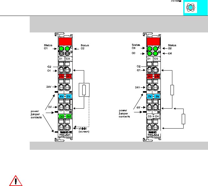
Digital Outputs (Standard)
PN 750-501...504, 516, 519
Technical description:
The power supply is provided by a series-connected supply module for the respective operating voltage. Power connections are made automatically from module to module via the internal P.J.C.s when snapped onto the DIN rail.
Attention:
The lowest power jumper contact is not carried out for some modules (e.g. 4-channel)! A module which needs all contacts (e.g. 2 channel digital) may not be connected to the right hand side of modules which do not have 3 power jumper contacts (e.g. 4 channel modules).
For the digital outputs (without diagnostic) four-conductor devices (V+; 0 V; signal; ground) are standard. In case of 12 mm wide 4-channel digital output modules it is not possible to use 4-conductor devices. 4 signal outputs, 2xV+ and 2x0V are provided. All digital outputs are short-circuit protected.
In case of overloads a supply module with fuse (750-601) must be connected on the line side to protect the output modules.
The module 750-516 is low-side switching. The indicated output values have been determined for 100% duty cycle. However, in case of the 2 A versions it is possible to operate single channels at higher load currents, however always verify that the total current does not exceed 3.5 A per module. Example: 2x2A (standard); 1x3.0A; 1x0.5A (total current: 3.5 A) The standard numerical assignment for bus operations is from left to right, starting with the LSB. The positions of the different I/O modules in the configured node/station are selectable by the user. A block type configuration is not necessary.The Output module can be connected to all buscouplers of the WAGOÇI/OÇSYSTEM.
Digital Outputs 750-501...504,516, 519 |
1 |
:$*2Ç, 2Ç6<67(0
Technical Data:
Item Number 750-
Number of outputs
Kind of load
Nominal voltage
Output current (DC)
Current consumption (internal)
Isolation
Internal bit width
Configuration
Operating temperature
Wire connection
Dimensions (mm)WxHxL
Item Number 750-
Number of outputs
Kind of load
Nominal voltage
Output current (DC)
Current consumption (internal)
Isolation
Internal bit width
Configuration
Operating temperature
Wire connection
Dimensions (mm)WxHxL
*) low-side switching
Item Number 750-
Number of outputs
Kind of load
Nominal voltage
Output current (DC)
Current consumption (internal)
Isolation
Internal bit width
Configuration
Operating temperature
Wire connection
Dimensions (mm)WxHxL
|
|
|
|
|
|
|
|
|
|
|
|
|
|
|
|
|
|
|
|
|
|
|
|
|
|
|
|
501 |
|
502 |
|
|
||
2 |
|
|
|
|
|
|
resistive, inductive, lamps |
|
|
|
|
|
|
24V DC (-15% / +20%) |
|
|
|
|
|
|
0,5 A |
|
2 A |
|
|
||
7 mA |
|
|
|
|
|
|
|
|
|
|
|
|
|
500 V system / power supply
2
without address or configuration adjustment
0°C....+55°C
CAGE CLAMP; 0,08 to 2,5mm2
12 x 64* x 100 (*from upper edge of the carrier rail)
504 |
516*) |
4
resistive, inductive, lamps
24V DC (-15% / +20%)
0,5 A
15 mA
500 V system / power supply
4
without address or configuration adjustment
0°C....+55°C
CAGE CLAMP; 0,08 to 2,5mm2
12 x 64* x 100 (*from upper edge of the carrier rail)
519
4
resistive, inductive, lamps
5 V DC
20 mA
16 mA
500 V system / power supply
4
without address or configuration adjustment
0°C....+55°C
CAGE CLAMP; 0,08 to 2,5mm2
12 x 64* x 100 (*from upper edge of the carrier rail)
Digital Outputs 750-501...504,516, 519 |
2 |
:$*2Ç, 2Ç6<67(0