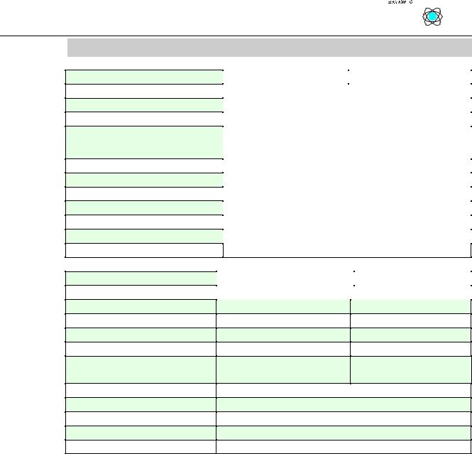
Материал: m013800e
Technical Data:
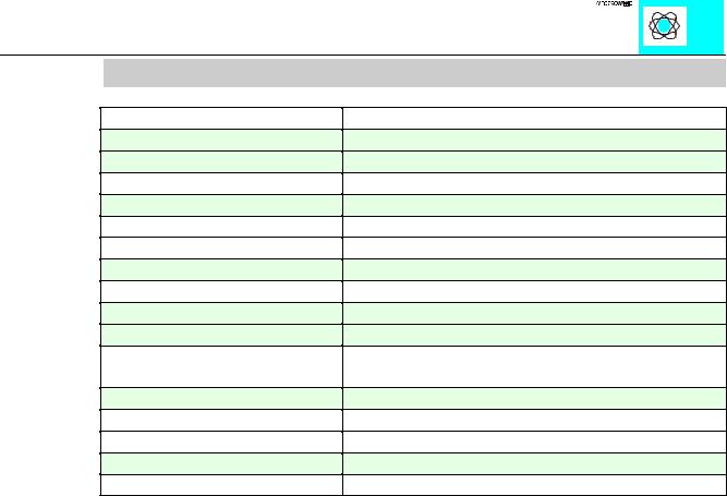
Part Number 750-
Number of outputs
Current consumption (internal)
Nominal voltage
Load type
Output current
Pulse frequency
Duty cycle
Resolution
Isolation
Configuration
Current Consumption (field side)
Internal bit width per channel
Operating temperature
Wire connections
Dimension (mm)BxHxT
Preset Frequency
511
2
70 mA typical (internal)
24V DC (-15% +20%)
ohmic, inductive
0.1 A, short circuit protected
1 Hz...20kHz
0%...100% (Ton > 750 ns, Toff > 500 ns)
10 Bit max.
500 V system/power Supply
none, optional with software parameter
15 mA typ.
16 Bit Data + 8 Bit Control/Status
0°C....+55°C
CAGE CLAMP; 0.08 to 2.5mm2
12 x 64* x 100 (*from upper edge of the carrier rail)
250 Hz Switching Frequency
Pulsewidth Module 750-511 |
2 |
:$*2Ç, 2Ç6<67(0
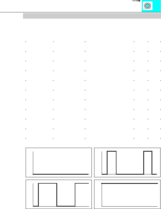
Formation of on/off times
The programming of the on/off times occur with the resolution of 10 bits. The five LSB of the 16 bit value can be zeros or one. The MSB will hold the sign and is preset to the null state.
Duty Cycle |
Increments |
Binary |
|
|
|
% |
|
Value |
Hex. |
Dec. |
|
100 |
1023 |
0111 1111 |
1111 1111 |
7F FF |
32767 |
|
|
|
|
|
|
100 |
1023 |
0111 1111 |
1111 0000 |
7F E0 |
32752 |
|
|
|
|
|
|
50 |
511 |
0011 1111 |
1111 1111 |
3F FF |
16383 |
|
|
|
|
|
|
25 |
255 |
0001 1111 |
1111 1111 |
1F FF |
8191 |
|
|
|
|
|
|
12.5 |
127 |
0000 0001 |
0000 0000 |
01 00 |
256 |
|
|
|
|
|
|
0.1955 |
2 |
0000 0000 |
0100 0000 |
00 40 |
16 |
|
|
|
|
|
|
0.0977 |
1 |
0000 0000 |
0010 0000 |
00 20 |
32 |
|
|
|
|
|
|
0 |
0 |
0000 0000 |
0001 1111 |
00 1F |
31 |
|
|
|
|
|
|
0 |
0 |
0000 0000 |
0000 0000 |
0 |
0 |
|
|
|
|
|
|
Table 1: Value Formation
0%
24V
0V |
t |
|
|
24V |
50% |
|
|
0V |
t |
|
24V |
25% |
|
|
0V |
t |
|
|
24V |
100% |
|
0V
t
Ill. 1: On/Off time relationships for Table 1.
Pulsewidth Module 750-511 |
3 |
:$*2Ç, 2Ç6<67(0
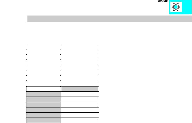
Process Image Formation for ModBus
The process image of the 750-511 appears with 6 bytes of input and 6 bytes of output data. The byte allocation for the preset duty cycle has the following modes of formation: Output values:
|
|
Function |
|
D0 |
|
Control Byte |
|
D1 |
|
Output Byte 1 |
|
D2 |
|
Output Byte 0 |
|
D3 |
|
reserved |
|
D4 |
|
Output Byte 3 |
|
D5 |
|
Output Byte 2 |
|
Input values:
D0
D1
D2
D3
D4
D5
Out(In)put byte 0 Out(In)put byte 1
Function
Status Byte
Input Byte 1
Input Byte 0
reserved
Input Byte 3
Input Byte 2
Low Byte
High Byte
Pulsewidth Module 750-511 |
4 |
:$*2Ç, 2Ç6<67(0
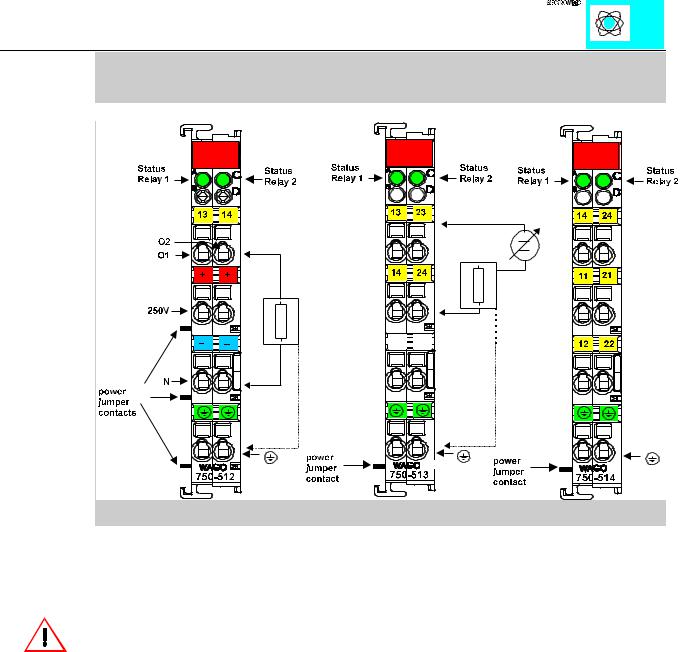
Digital Outputs (Relay)
PN 750-512...514, 517
Technical description:
The power supply for the relay coils is not made via the power jumper contacts but directly from the electronics. The respective output contacts of the switching element are therefore always positioned at the field side.
Attention:
The lowest power jumper contact is not carried out for some modules (e.g. 4-channel)! A module which needs all contacts (e.g. 2 channel digital) may not be connected to the right hand side of modules which do not have 3 power jumper contacts (e.g. 4 channel modules).
Version 1: non-floating (750-512)
The power supply is made via a series-connected supply terminal block for the respective operating voltage. Power connections are made automatically from module to module when snapped onto the DIN rail. One termination point of these contacts must be directly connected to the power supply.
Version 2: isolated outputs (750-513, 750-514)
These I/O modules are not provided with integrated power jumper contacts. Care should be taken to supply each isolated module with separate power supply connections.
The standard numerical assignment for Bus operation is from left to right, starting with the LSB. The positions of the different inputs in the configured station are via the user’s choice. A block type configuration is not necessary. The output module can be connected to all buscouplers of the WAGOÇI/OÇSYSTEM.
Digital Outputs 750-512-514,517 |
1 |
:$*2Ç, 2Ç6<67(0
Technical Data:
Item Number 750-
Type of contact
Current consumption (internal)
Switching voltage
Switching power
Switching current
Isolation
Internal bit width
Configuration
Operating temperature
Wire connection
Dimensions (mm)WxHxL
Item Number 750-
Type of contact
Current consumption (internal)
Switching voltage
Switching power
Switching current
Isolation
Internal bit width
Configuration
Operating temperature
Wire connection
Dimensions (mm)WxHxL
*ohmic load 1)in design
|
|
|
|
|
|
|
|
|
|
|
|
|
|
|
|
|
|
|
|
|
|
|
|
|
|
|
|
|
|
|
|
|
|
|
|
|
|
|
|
512 |
|
|
|
513 |
|
|
|
||
|
2 make contacts |
||||||||
|
|
100 mA max. |
|
||||||
30 V DC; 250V AC |
|||||||||
|
|
60 W; 500 VA |
|
||||||
cos |
ρ |
max |
=0,4, L/Rmax=7 ms |
|
|||||
|
|
2 A AC/ DC |
|
||||||
4 kV system/power supply |
|||||||||
|
|
2 |
|
|
|
|
|
||
without address or configuration adjustment |
|
||||||||
|
|
0°C....+55°C |
|||||||
CAGE CLAMP; 0.08 to 2.5mm2 |
|
||||||||
12 x 64* x 100 (*from upper edge of the carrier rail)
514 |
|
5171) |
|
2 changeover |
|
70 mA max.
30 V DC; 125 V AC
30 W; 62.5 VA
0.5A AC/ 1 A DC
1.5kV system/power supply
80 mA max.
250 V AC
1500 VA*
1 A AC
4 kV system/ power supply
2
without address or configuration adjustment
0°C....+55°C
CAGE CLAMP; 0.08 to 2.5mm2
12 x 64* x 100 (*from upper edge of the carrier rail)
Digital Outputs 750-512-514,517 |
2 |
:$*2Ç, 2Ç6<67(0