Материал: m013802e_b

5.3.3 Configuration function
The following registers can be read, in order to determine the configuration of the connected modules:
Register |
Designation |
Access |
Length |
Default |
Description |
||
address |
|
|
(word) |
|
|
|
|
0 x 1022 |
CnfLen. AnalogOut |
read |
4++ |
pu |
Number of I/O bits with the process |
||
|
|
|
|
|
data words of the outputs |
||
|
|
|
|
|
|
||
0 x 1023 |
CnfLen.AnalogInp |
read |
3++ |
pu |
Number of I/O bits with the process |
||
|
|
|
|
|
data words of the inputs |
||
|
|
|
|
|
|
||
0 x 1024 |
CnfLen.DigitalOut |
read |
2++ |
pu |
Number of I/O bits with the process |
||
|
|
|
|
|
data bits of the outputs |
||
|
|
|
|
|
|
||
0 x 1025 |
CnfLen.DigitalInp |
read |
1 |
pu |
Number of I/O bits with the process |
||
|
|
|
|
|
data bits of the inputs |
||
|
|
|
|
|
|
||
0 x 1026 |
slaveAdr |
read |
1 |
pu |
Current node address. The address |
||
|
|
|
|
|
is read when switching on the voltage |
||
|
|
|
|
|
supply. |
|
|
|
|
|
|
|
|
||
0 x 1027 |
Settings |
read |
1 |
pu |
The current settings are saved here. |
||
These are interrogated when |
|||||||
|
|
|
|
|
|||
|
|
|
|
|
switching on the voltage supply. |
||
|
|
|
|
|
D0-D2: |
Baud rate |
|
|
|
|
|
|
D3-D4: |
Byte Frame |
|
|
|
|
|
|
D5: |
Data Length 8/7 Bit |
|
|
|
|
|
|
D6: |
Not in use |
|
|
|
|
|
|
D7: |
Not in use |
|
|
|
|
|
|
D8-D10: |
End of Frame Time |
|
|
|
|
|
|
D11: |
RTU/ASCII mode |
|
|
|
|
|
|
D12: |
Error Check |
|
|
|
|
|
|
|
switched off/switched on |
|
|
|
|
|
|
D13: |
Extended Functions |
|
|
|
|
|
|
|
switched off/switched on |
|
|
|
|
|
|
D14: |
Watchdog |
|
|
|
|
|
|
|
switched off/switched on |
|
|
|
|
|
|
D15: |
Not in use |
|
|
|
|
|
|
|
||
Table 5.49: Configuration function |
|
|
pu: Default value when switching voltage on |
||||
70 |
MODBUS / Configuration |
15.12.99

5.3.4 Firmware information
These registers are used to read out information about the coupler or controller firmware.
Register |
Designation |
Access |
Length |
Default |
Description |
address |
|
|
(word) |
|
|
|
|
|
|
|
|
0x2010 |
Revison, |
read |
1 |
pu/co - |
Firmware version (256* major + minor) |
|
INFO_REVISION |
|
|
|
e.g.: V2.5 = 0x0205 |
|
|
|
|
|
|
0x2011 |
Series code, |
read |
1 |
pu/co - |
WAGO series number: |
|
INFO_SERIES |
|
|
|
750 for WAGO-I/O System |
|
|
|
|
|
|
0x2012 |
Item number, |
read |
1 |
pu/co - |
WAGO order number: |
|
INFO_ITEM |
|
|
|
312, 314, 315, 316 for coupler, |
|
|
|
|
|
812, 814, 815, 816 for controller |
|
|
|
|
|
|
0x2013 |
Major sub item code, |
read |
1 |
pu/co - |
Extended WAGO order number. |
|
INFO_MAJOR |
|
|
|
Is used for special firmware versions or |
|
|
|
|
|
settings: |
|
|
|
|
|
0xFFFF for coupler/controller. |
|
|
|
|
|
|
0x2014 |
Minor sub item code, |
read |
1 |
pu/co - |
Extended WAGO order number. |
|
INFO_MINOR |
|
|
|
Is used for special firmware versions or |
|
|
|
|
|
settings: |
|
|
|
|
|
0xFFFF for coupler/controller. |
|
|
|
|
|
|
0x2020 |
Description, |
read |
128 |
pu/co - |
Brief description for this |
|
INFO_DESCRIPTION |
|
|
|
coupler/controller, max. 255 characters. If |
|
|
|
|
|
not available the value 0xFF appears. |
|
|
|
|
|
|
0x2021 |
Description, |
read |
16 |
pu/co - |
Details of the manufacture time of the |
|
INFO_TIME |
|
|
|
firmware version, max. 31 characters. If |
|
|
|
|
|
not available the value 0xFF appears. |
|
|
|
|
|
|
0x2022 |
Description, |
read |
16 |
pu/co - |
Details of manufacture date of the |
|
INFO_DATE |
|
|
|
firmware version, max. 31 characters. If |
|
|
|
|
|
not available the value 0xFF appears. |
|
|
|
|
|
|
0x2023 |
Description, |
read |
32 |
pu/co - |
Details of the company and user of the |
|
INFO_LOADER_INFO |
|
|
|
firmware programming unit, max. 63 |
|
|
|
|
|
characters. If not available the value |
|
|
|
|
|
0xFF appears. |
|
|
|
|
|
|
Table 5.50: Firmware information |
|
pu: Default value when switching voltage on, co: Constant |
|||
MODBUS / Configuration |
71 |
15.12.99

5.3.5 General registers
The constants saved here can be used to test the communication with the master.
Register |
Designation |
Access |
Length |
Default |
Description |
address |
|
|
(word) |
|
|
|
|
|
|
|
|
0x2000 |
Zero, GP_ZERO |
read |
1 |
pu/co |
Constant with zero. |
|
|
|
|
0x0000 |
|
|
|
|
|
|
|
0x2001 |
Units, GP_ONES |
read |
1 |
pu/co |
Constant with units. Is -1 if declared as ”signed |
|
|
|
|
0xFFFF |
int” or MAXVALUE if ”unsigned int”. |
|
|
|
|
|
|
0x2002 |
1,2,3,4, GP_1234 |
read |
1 |
pu/co |
Constant value to test whether high and low |
|
|
|
|
0x1234 |
bytes are changed over (Intel/Motorola format). |
|
|
|
|
|
Should appear in the master as 0 x 1234. If |
|
|
|
|
|
0 x 3412 appears the high and low byte must be |
|
|
|
|
|
changed over. |
|
|
|
|
|
|
0x2003 |
Mask1, GP_AAAA |
read |
1 |
pu/co |
Constant to see if all bits are present. Is used |
|
|
|
|
0xAAAA |
together with register 0 x 2004. |
|
|
|
|
|
|
0x2004 |
Mask2, GP_5555 |
read |
1 |
pu/co |
Constant to see if all bits are present. Is used |
|
|
|
|
0x5555 |
together with register 0 x 2003. |
|
|
|
|
|
|
0x2005 |
Largest positive |
read |
1 |
pu/co |
Constant, to check the arithmetic. |
|
number, |
|
|
0x7FFF |
|
|
GP_MAX_POS |
|
|
|
|
|
|
|
|
|
|
0x2006 |
Largest negative |
read |
1 |
pu/co |
Constant, to check the arithmetic. |
|
number, |
|
|
0x8000 |
|
|
GP_MAX_NEG |
|
|
|
|
|
|
|
|
|
|
0x2007 |
Largest semi-positive |
read |
1 |
pu/co |
Constant, to check the arithmetic. |
|
number, |
|
|
0x3FFF |
|
|
GP_HALF_POS |
|
|
|
|
|
|
|
|
|
|
0x2008 |
Largest semi- |
read |
1 |
pu/co |
Constant, to check the arithmetic. |
|
negative number, |
|
|
0x4000 |
|
|
GP_HALF_NEG |
|
|
|
|
|
|
|
|
|
|
Table 5.51: General registers |
|
|
pu: Default value when switching on voltage ; co: constant |
||
72 |
MODBUS / Configuration |
15.12.99
6 Start-Up and Diagnosis
6.1 Run-up and error indications
After the supply voltage connection the coupler/controller checks all the functions of its components and the communication interface. The configuration of the I/O modules is then determined. The 'I/O ERR' LED is blinking during the run-up time. The coupler/controller enters then the "fieldbus start" status after the successful run-up. The green "I/O RUN" LED indicates this status. If an error occurs, the red "I/O ERR" goes on blinking in a low frequency. The various types of error are indicated via up to 3 different flash sequences.
Display functions of the 'I/O ERR' LED:
1. Coupler/controller’s start-up phase after the supply voltage connection
2. Introduction of the error indication
3. Error code
(number of flash cycles 2nd flash sequence)
4.Error argument
(Number of flash cycles 3rd flash sequence)
Fig. 6.1: LED fieldbus start and error indication
1st flash sequence |
1st pause |
2nd flash sequence |
2nd pause |
3rd flash sequence |
2nd flash sequence |
3rd flash sequence |
Meaning |
|
|
|
Error code |
Error argument |
|
|
|
|
1 |
0 |
EEPROM check sum error |
|
|
|
|
1 |
Internal storage overflow for the inline code |
|
|
|
|
2 |
Unknown data type |
|
|
|
2 |
0 |
Programmed process image assignement is not plausible |
|
|
|
|
N (N>0) |
Error in table comparison I/O module N (programmed |
|
|
configuration), passive modules as well as potential supply modules |
|
|
are not taken into account |
|
|
|
3 |
0 |
I/O module(s) has (have) identified the internal bus command as |
|
|
wrong |
|
|
|
4 |
0 |
Data error at internal bus or internal bus break at coupler / controller |
|
|
|
|
N (N>0) |
Internal bus interrupted after N module |
|
|
|
5 |
N |
Internal bus error in the communication with N module |
|
|
|
Table 6.1: Error diagnosis, nodes
MODBUS / Start-up and diagnosis |
73 |
15.12.99
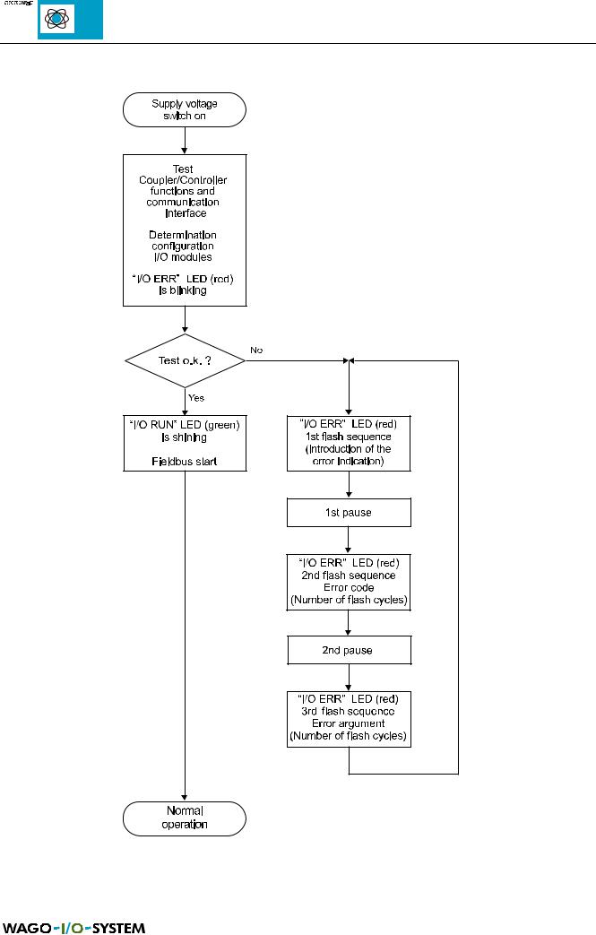
Fig. 6.2: Run-up coupler/controller
74 |
MODBUS / Start-up and diagnosis |
15.12.99