Материал: m012900e
I/O modules • 107
Counter modules 750-404/000-001
4.2.1.1.4Variation
Counter with enable input 750-404/000-001
Technical description
The counter module also can be ordered as counter with enable input (750404/000001).
The counter begins processing with pulses at the CLOCK input. The changes from 0 V to 24 V are counted.
The counting is enabled if the GATE (U/D)terminal is an open circuit input or 0V. To disable processing, the GATE (U/D)input is to be set to 24 V DC.
The data format of the module is 4 bytes data and a control/status byte. The module is a 32 Bit counter. The format of input and output data is the same as 750-404.
The counter module can operate with all WAGO-I/O-SYSTEM bus-couplers (except for the economy type).
Modular I/O System
ETHERNET TCP/IP

108 • I/O modules
Counter modules 750-404/000-002
4.2.1.1.5Variation
Peak Time Counter 750-404/000-002
Technical description
The counter module also can be ordered as peak time counter with 750-404/000-002.
This description is only intended for hardware version X X X X 0 0 0 1- - - -. The serial number can be found on the right side of the module.
The counter begins processing with pulses at the CLOCK input. The changes from 0 V to 24 V are counted.
The counter counts up if the input U/D is set at 24 V. With an open circuit input or 0 V the counter counts backwards.
The two bottom contacts each include another output. These outputs are activated through bits in the control byte.
The high states of the input and output channels are each indicated by a LED. The counter module can operate with all WAGO-I/O-SYSTEM bus-couplers (except for the economy type).
Organization of the input and output data:
The counter begins processing with pulses at the CLOCK input and counts the pulses in a special time span. The time span is given as 10 s.
The state of the counter is stored in the process image until the next period. After the recording the counting starts again at 0.
The activation of the counting and the synchronization with the SPS is made by a handshake in the control and status byte.
The end of the counting period and thus the new process data is signaled by a toggle bit in the status byte.
The control byte has the following bits:
Bit |
7 |
Bit |
6 |
Bit 5 |
Bit |
4 |
Bit 3 |
Bit 2 |
Bit |
1 |
Bit |
0 |
|
|
|
|
|
|
|
|
|
|
|
|
|
0 |
|
0 |
|
Start of the |
0 |
|
Output |
Output |
0 |
|
0 |
|
|
|
|
|
periodic |
|
|
value at |
value at |
|
|
|
|
|
|
|
|
counting |
|
|
output O2 |
output O1 |
|
|
|
|
The status byte has the following bits:
Bit |
7 |
Bit |
6 |
Bit 5 |
Bit |
4 |
Bit 3 |
Bit 2 |
Bit 1 |
Bit 0 |
|
|
|
|
|
|
|
|
|
|
|
0 |
|
0 |
|
Couting star- |
0 |
|
actual |
Actual |
actual si- |
Togglebit |
|
|
|
|
ted |
|
|
signal at |
signal at |
gnal at input |
for end of |
|
|
|
|
|
|
|
output O2 |
output O1 |
V/R |
the record |
Modular I/O System
ETHERNET TCP/IP

|
I/O modules • 109 |
|
Counter modules 750-404/000-003 |
|
|
4.2.1.1.6 Variation |
|
Frequency Counter Module |
750-404/000-003 |
Technical description
The counter module also can be ordered as frequency counter module with 750-404/000-003.
The counter module 750-404/000-003 measures the period of the 24 V DC input signal at the CLOCK terminal and converts it into a corresponding frequency value. The measurement is enabled if the GATE terminal is an open circuit input or 0V. To disable processing, the GATE input is to be set to 24 V DC.
The terminals O1 and O2 work as binary outputs. Each output can be activated via specific bits in the CONTROL byte.
The high states of the input and output channels are each indicated by a LED.
To recognize low frequency or near zero frequency signals, the maximum time between two data updates is parameterizable.
Modular I/O System
ETHERNET TCP/IP
110 • I/O modules
Counter modules 750-404/000-003
Technical Data:
Item-No.:
Number of outputs
Number of counters
Output current
Input current (internal)
Voltage via power jumper contacts
Signal voltage (0)
Signal voltage (1)
Min. Pulse width
Input current
Voltage drop
Internal Bit width
Operating temperature
Wire connection
Dimensions (mm) WxHxL
Max. Frequency Range
Integration time = 1 period
Integration time = 4 periods
Integration time = 16 periods
Measuring Error using the max. Frequency Range
Range 0.1 Hz |
- |
8 kHz |
|
|
|
|
|
Range |
0.25 Hz - |
32 kHz |
|
|
|
|
|
Range |
1 Hz |
- |
100 kHz |
|
|
|
|
|
|
|
|
Measurements in a
Lower Frequency Range*)
Integration time = 1 period
Integration time = 4 periods
Integration time = 16 periods
Measuring Error using the
lower Frequency Range*)
Range |
0.1 |
Hz - 100 Hz |
|
|
|
|
|
Range |
1 Hz - |
1 kHz |
|
|
|
|
|
Range |
10 |
Hz - |
10 kHz |
|
|
|
|
750-404/000-003
2
1
0.5A (short-circuit protected)
80mA max. at DC 5V
DC 24V (-15%/+20%)
DC -3V ... 5V
DC 15V ... 30V
10µs
5mA typ.
DC 0.6V max. at 0.5A
32 Bit Data + 8 Bit control/status
0°C....+55°C
CAGE CLAMP ; 0.08 mm2 - 2.5 mm2, AWG 28 – 14, 8 – 9 mm Stripped length
12 x 64* x 100 (*from upper edge of carrier rail)
0.1 Hz - 8 kHz, Resolution 0.001Hz
0.25 Hz - 32 kHz, Resolution 0.01Hz
1 Hz - 100 kHz, Resolution 0.1Hz (1Hz)
<± 1%
<± 1.5 %
<± 1.5 %
0.1Hz - 100 Hz, Resolution 0.001Hz 1 Hz - 1 kHz, Resolution 0.01Hz
10 Hz - 10 kHz, Resolution 0.1Hz (1Hz)
<± 0.05%
<± 0.05 %
<± 0.2 %
*) For Measurements in a lower frequency range, the measuring error is lower than the measuring error using the maximum frequency range.
Modular I/O System
ETHERNET TCP/IP
I/O modules • 111
Counter modules 750-404/000-003
Functional description
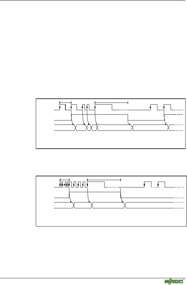
The counter module acquires the time between one or more rising edges of the CLOCK input signal and calculates the frequency of the applied signal.
The calculation and process image update are initiated every 1st , every 4th or every 16th rising edge depending on the integration time selected via the CONTROL byte. The first detection of a rising edge starts the cyclic period measurement and cannot provide a valid frequency value. In this case the module will send 0xFFFFFFFFH for input information. The same input value is returned when a static high or static low signal is applied to the CLOCK input.
If there are no signal changes seen at the CLOCK input, the module can be forced to update the process image after defined parameterizable time spans. In this state the module will send the non valid value 0xFFFFFFFFH too.
The following figures illustrate a process data cycle.
TP |
T1 |
INPUT FREQ
DATA VALID
PROCESS DATA 0xFFFFFFFF |
D0..D3 |
D0..D3 |
0xFFFFFFFF |
D0..D3 |
|
D0..D3D0..D3 |
|
|
|
D0..D3Input Data
T= 1/f current period
P
T1 Maximum data hold time (parameterizable)
Timing diagram for process data update sequence (Integration time = 1 period)
4 TP |
|
T1 |
|
INPUT FREQ |
|
|
|
DATA VALID |
|
|
|
PROCESS DATA 0xFFFFFFFF |
D0..D3 |
D0..D3 |
0xFFFFFFFF |
D0..D3 Input Data
T= 1/f current period
P
T1 Maximum data hold time (parameterizable)
Timing diagram for process data update sequence (integration time = 4 periods)
Modular I/O System
ETHERNET TCP/IP