Материал: m012900e
Fieldbus controller 750-842 • 67
Data exchange
In addition, the controller offers further memory spaces which cannot be accessed from the fieldbus side:
RAM |
The RAM memory is used to create variables not required for |
|
communication with the interfaces but for internal processing, |
|
such as for instance computation of results. |
|
|
Retentive memory
Code memory
The retentive memory is non volatile memory, i.e. all values are retained following a voltage failure. The memory management is automatic. In this memory area, flags for the IEC 61131-3 program are filed together with variables without memory space addressing or variables which are explicitly defined with "var retain".
Note
The automatic memory management can cause a data overlap. For this reason, we recommend not to use a mix of flags and retain variables.
The IEC 61131-3 program is filed in the code memory. The code memory is a flash ROM. Once the supply voltage is applied, the program is transmitted from the flash to the RAM memory. After a successful start-up, the PFC cycle starts when the operating mode switch is turned to its upper position or by a start command from WAGO-I/O-PRO 32.
3.2.5.2Addressing
3.2.5.2.1 Addressing the I/O modules
The arrangement of the I/O modules in a node is optional.
When addressing, first of all the complex modules (modules occupying 1 or more bytes) are taken into consideration in accordance with their physical order behind the fieldbus controller. As such, they occupy the addresses beginning with word 0.
Following this, the data of the other modules follow - grouped into bytes - (modules occupying less than 1 byte). These are filled byte-by-byte according to their physical order. As soon as a full byte is occupied by the bit oriented modules, the next byte starts automatically.
Note
For the number of input and output bits or bytes of the individually connected bus modules please refer to the corresponding descriptions of the bus modules.
Note
Changing a node could result into a new structure of the process image. Also the addresses of the process data will change. When adding modules, the process data of all previous modules have to be taken into account.
Modular I/O System
ETHERNET TCP/IP
68 • Fieldbus controller 750-842 Data exchange
Data width • :RUG FKDQQHO
Analog input modules
Analog output modules
Input modules for thermal elements
Input modules for resistance sensors
Pulse width output modules
Interface module
Up/down counter
I/O modules for angle and path measurement
Data width = 1 Bit / channel
Digital input modules
Digital output modules
Digital output modules with diagnosis (2 Bit / channel)
Power supply modules with fuse holder / diagnosis
Solid State power relay
Relay output modules
Table 3.4: I/O module data width
3.2.5.2.2 Address range
Address range for I/O module data:
|
Data |
|
Address |
|
|
|
|
|
|
|
|
|
|
||
|
Bit |
|
0.0 ... |
0.8... |
1.0 ... |
1.8... |
|
..... |
|
254.0 ... |
254.8...2 |
255.0 ... |
255.8... |
|
|
|
|
0.7 |
0.15 |
1.7 |
1.15 |
|
|
|
254.7 |
54.15 |
255.7 |
255.15 |
|
||
|
Byte |
|
0 |
1 |
2 |
3 |
|
..... |
|
508 |
509 |
510 |
511 |
|
|
|
|
|
|
|
|
|
|
|
|
|
|
|
|
|
|
|
Word |
|
0 |
|
1 |
|
|
..... |
|
254 |
|
255 |
|
|
|
|
|
|
|
|
|
|
|
|
|
|
|
|
|
|
|
|
DWord |
|
0 |
|
|
|
|
..... |
|
127 |
|
|
|
|
|
|
|
|
|
|
|
|
|
|
|
|
|
|
|
|
|
|
Table 3.5: Address range for the I/O module data |
|
|
|
|
|
|
||||||||
Address range for fieldbus data: |
|
|
|
|
|
|
|
|
|||||||
|
Data |
|
Address |
|
|
|
|
|
|
|
|
|
|
||
|
Bit |
|
256.0 |
256.8 |
257.0 |
257.8 |
|
..... |
|
510.0 |
510.8 |
511.0 |
511.8 |
|
|
|
|
... |
... |
... |
... |
|
|
|
... |
... |
... |
... |
|
||
|
|
|
256.7 |
256.15 |
257.7 |
257.15 |
|
|
|
510.7 |
510.15 |
511.7 |
511.15 |
|
|
|
|
|
|
|
|
||||||||||
|
Byte |
|
512 |
513 |
514 |
515 |
|
..... |
|
1020 |
1021 |
1022 |
1023 |
|
|
|
|
|
|
|
|
|
|
|
|
|
|
|
|
|
|
|
Word |
|
256 |
|
257 |
|
|
..... |
|
510 |
|
511 |
|
|
|
|
|
|
|
|
|
|
|
|
|
|
|
|
|
|
|
|
DWord |
|
128 |
|
|
|
|
..... |
|
255 |
|
|
|
|
|
|
|
|
|
|
|
|
|
|
|
|
|
|
|
|
|
|
|
|
|
|
|
|
|
|
|
|
|
|
|||
|
Table 3.6: Address range for the fieldbus data |
|
|
|
|
|
|
||||||||
Address range for flags: |
|
|
|
|
|
|
|
|
|
|
|||||
|
Data |
|
Address |
|
|
|
|
|
|
|
|
|
|
||
|
Bit |
|
0.0 ... |
0.8... |
1.0... |
1.8... |
|
..... |
|
4094.0.. |
4094.8.. |
4095.0 ... |
4095.8... |
|
|
|
|
0.7 |
0.15 |
1.7 |
1.15 |
|
|
|
4094.7 |
4094.15 |
4095.7 |
4095.15 |
|
||
|
Byte |
|
0 |
1 |
2 |
3 |
|
..... |
|
8188 |
8189 |
8190 |
8191 |
|
|
|
|
|
|
|
|
|
|
|
|
|
|
|
|
||
|
Word |
|
0 |
|
1 |
|
|
..... |
|
4094 |
|
4095 |
|
|
|
|
|
|
|
|
|
|
|
|
|
|
|
|
|
||
|
DWord |
|
0 |
|
|
|
|
..... |
|
2047 |
|
|
|
|
|
|
|
|
|
|
|
|
|
|
|
|
|
|
|
||
Table 3.7: Address range for the flags
The register functions are located in address 0x1000 and can be addressed analog with the implemented MODBUS function codes (read/write).
Modular I/O System
ETHERNET TCP/IP
Fieldbus controller 750-842 • 69
Data exchange
3.2.5.2.3 Absolute addresses
The direct display of individual memory cells (absolute addresses) in accordance with IEC 61131-3 is made using special character strings in accordance with the following table:
|
Position |
|
Character |
|
Designation |
|
Comments |
|
|
1 |
|
% |
|
Starts absolute address |
|
|
|
|
2 |
|
I |
|
Input |
|
|
|
|
|
|
Q |
|
Output |
|
|
|
|
|
|
|
|
|
|
||
|
|
|
|
|
|
|
||
|
|
|
M |
|
Flag |
|
|
|
|
|
|
|
|
|
|
||
|
|
|
|
|
|
|
||
|
|
|
|
|
|
|
|
|
|
3 |
|
X* |
|
Single bit |
|
Data width |
|
|
|
|
B |
|
Byte (8 Bits) |
|
|
|
|
|
|
|
|
|
|
||
|
|
|
W |
|
Word (16 Bits) |
|
|
|
|
|
|
|
|
|
|
||
|
|
|
|
|
|
|
||
|
|
|
D |
|
Double word (32 Bits) |
|
|
|
|
|
|
|
|
|
|
||
|
|
|
|
|
|
|
||
|
|
|
|
|
|
|
|
|
|
4 |
|
|
|
Address |
|
|
|
|
|
|
|
|
|
|
|
|
* The character ‘X’ for bits can be deleted
Table 3.8: Absolute addresses
Note
Enter the absolute address character strings without blanks!
Example: Absolute addresses for input:
%IX14. |
.15 |
.14 |
.13 |
.12 |
.11 |
.10 |
.9 |
.8 |
.7 |
|
.6 |
.5 |
.4 |
.3 |
.2 |
.1 |
.0 |
%IB29 |
|
|
%IB28 |
|
|
|
|
|
|
|
|||||||
%IW14
%IDW7
* The character ‘X’ for single bits can be deleted
Table 3.9: Example for input absolute addresses
Address calculation (depending upon the word address):
Bit address: |
word address .0 to .15 |
|
Byte address: |
1. |
Byte: 2 x word address |
|
2. |
Byte: 2 x word address + 1 |
Dword address: |
|
|
word address (even numbers) / 2 |
or |
word address (uneven numbers) / 2, rounded off |
Modular I/O System
ETHERNET TCP/IP
70 • Fieldbus controller 750-842
Data exchange
3.2.5.3Data exchange between master and I/O modules
The data exchange between the MODBUS master and the I/O modules is made via the MODBUS functions implemented in the controller by reading and writing in bits or bytes.
The controller handles four different types of process data:
•Input words
•Output words
•Input bits
•Output bits
The word for word access to the digital input and output modules is made in accordance with the following table:
Digital inputs/ outputs
Prozess data
word
Byte
16. |
15. |
14. |
13. |
12. |
11. |
10. |
9. |
8. |
7. |
6. |
5. |
4. |
3. |
2. |
1. |
|
|
|
|
|
|
|
|
|
|
|
|
|
|
|
|
Bit |
Bit |
Bit |
Bit |
Bit |
Bit |
Bit |
Bit |
Bit |
Bit |
Bit |
Bit |
Bit |
Bit |
Bit |
Bit |
15 |
14 |
13 |
12 |
11 |
10 |
9 |
8 |
7 |
6 |
5 |
4 |
3 |
2 |
1 |
0 |
|
|
|
|
|
|
|
|
|
|
|
|
|
|
|
|
High-Byte |
|
|
|
|
|
|
Low-Byte |
|
|
|
|
|
|
||
D1 |
|
|
|
|
|
|
|
D0 |
|
|
|
|
|
|
|
Table 3.10: Allocation of digital inputs/outputs to process data word acc. Intel format
Adding 0x0200 to the MODBUS address permits to read back the outputs.
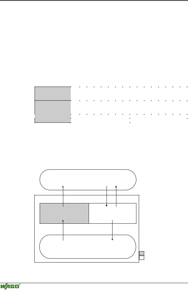
The register functions addressing can be by the means of the implemented MODBUS function codes (read/write). The individual register address is referenced instead of the address of a module channel.
MODBUS master |
||
0x000 |
0x000 |
|
|
(0x200) |
|
PII |
PIO |
|
0x0FF |
0x0FF |
|
(0x2FF) |
||
|
||
Inputs |
Outputs |
|
|
I/O modules |
|
|
PII = Process Input |
|
|
Image |
|
|
PIO = Process Output |
|
|
Image |
|
Programmable Fieldbus Controller
Fig. 3-27: Data exchange between MODBUS master and I/O modules |
g012929e |
Modular I/O System
ETHERNET TCP/IP
Fieldbus controller 750-842 • 71
Data exchange
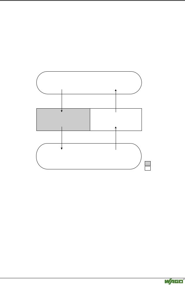
3.2.5.4Data exchange between PLC functionality (CPU) and I/O modules
Through absolute addresses, the PLC functionality (CPU) of the PFC can directly address the bus module data.
The PFC addresses the input data with absolute addresses. The data can then be processed, internally in the controller, through the IEC 61131-3 program, whereby the flags are filed in a permanent memory area. Following this, the linking results can be directly written in the output data via absolute addressing.
Inputs |
Outputs |
I/O modules |
750-4xx....6xx |
%IW0 |
%QW0 |
PII |
PIO |
%IW255 |
%QW255 |
Inputs |
Outputs |
PLC functionality (CPU)
PII = Process Input
Image
PIO = Process Output
Image
Programmable Fieldbus Controller
Fig. 3-28: Data exchange between PLC functionality (CPU) and I/O modules |
g012943e |
Modular I/O System
ETHERNET TCP/IP