Материал: m013209e
Structure of the inand output data for InterBus S (from firmware WF)
The module is a combined special function input and output module with 2 x 16 Bit inand output data.
Input
|
Description |
|
Word |
High |
Low |
n (Bit0-Bit15) |
Input byte0 |
Input byte1 |
n+1 (Bit16-Bit31) |
Input byte2 |
Input byte3 |
Output |
|
|
|
|
|
|
Description |
|
Word |
High |
Low |
n (Bit0-Bit15) |
Output byte0 |
Output byte1 |
n+1 (Bit16-Bit31) |
Output byte2 |
Output byte3 |
Attention:
For Interbus S the data is written in Motorola format (high Byte first). In connection with other fieldbus systems the Bytes in the data word are changed.
Attention:
The control byte allows the changing of the registers of the module. It must always be 0 in order to avoid a change in the registers. A wrong mapping can change the function of the module!
Data exchange module 750-654 |
5 |
:$*2Ç, 2Ç6<67(0
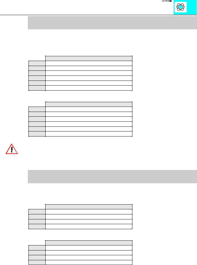
Structure of the inand output data for DeviceNet (from firmware 306V2.2)
The module has 6 Bytes input and output data in the Poll I/O data. Consumed (Tx for the Scanner) and produced (Rx for the Scanner) data size are each 6 Byte more.
Input
Byte Description
D0 Control byte
D1 Input byte1
D2 Input byte0
D3 Input byte4
D4 Input byte3
D5 Input byte2
Output
Byte Description
D0 Status byte
D1 Input byte1
D2 Input byte0
D3 Input byte4
D4 Input byte3
D5 Input byte2
Attention:
The control byte allows the changing of the registers of the module. It must always be 0 in order to avoid a change in the registers. A wrong mapping can change the function of the module!
Structure of the inand output data for DeviceNet (from firmware 306V3.0)
The module has 4 Bytes input and output data in the polled I/O data.
Input
Byte Description
D0 Input byte0
D1 Input byte1
D2 Input byte2
D3 Input byte3
Output
Byte Description
D0 Input byte0
D1 Input byte1
D2 Input byte2
D3 Input byte3
Data exchange module 750-654 |
5 |
:$*2Ç, 2Ç6<67(0

Structure of the inand output data for Modbus (from firmware V2.3)
The module is a combined special function input and output module with 2 x 16 Bit inand output data.
Input
|
Description |
|
Word |
High |
Low |
n (Bit0-Bit15) |
Input byte0 |
Input byte1 |
n+1 (Bit16-Bit31) |
Input byte2 |
Input byte3 |
Output |
|
|
|
|
|
|
Description |
|
Word |
High |
Low |
n (Bit0-Bit15) |
Output byte0 |
Output byte1 |
n+1 (Bit16-Bit31) |
Output byte2 |
Output byte3 |
Attention:
For Interbus S the data is written in Motorola format (high Byte first). In connection with other fieldbus systems the Bytes in the data word are changed.
Attention:
The control byte allows the changing of the registers of the module. It must always be 0 in order to avoid a change in the registers. A wrong mapping can change the function of the module!
Data exchange module 750-654 |
5 |
:$*2Ç, 2Ç6<67(0
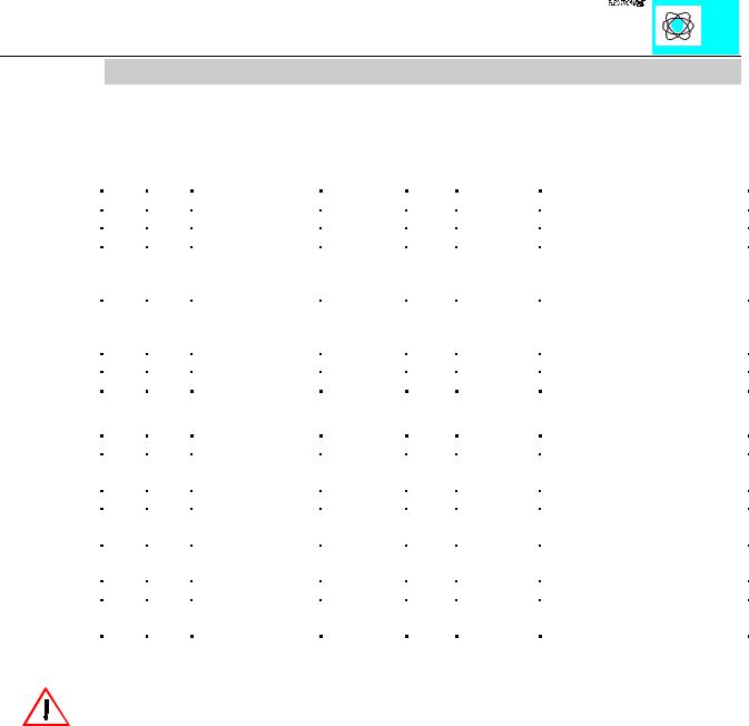
Structure of the inand output data for CanOpen (from firmware WI)
The module is in the list with Index 0x2400 (input) and Index 0x2500 (output). The module has 2 subindexes.
2 Byte special modules, Inputs
Idx |
|
SIdx |
|
Name |
|
Type |
|
Attrib. |
|
Default |
|
Description |
2400 |
|
0 |
|
special 2 byte input |
|
Unsigned8 |
|
ro |
|
none |
|
number of 2 Byte channels |
|
.... |
.... |
.... |
.... |
.... |
.... |
||||||
|
|
n |
|
Input byte0, Input |
|
Unsigned16 |
|
ro |
|
none, 0x0 |
|
1. and 2. Input byte |
|
|
|
|
byte1 |
|
|
|
|
|
for WD |
|
|
|
|
|
|
|
|
|
|
|
|
error |
|
|
|
|
n+1 |
|
Input byte2, Input |
|
Unsigned16 |
|
ro |
|
none, 0x0 |
|
3. and 4. Input byte |
|
|
|
|
byte3 |
|
|
|
|
|
for WD |
|
|
|
|
|
|
|
|
|
|
|
|
error |
|
|
|
.... |
.... |
.... |
.... |
.... |
.... |
||||||
|
|
0xFF |
|
0xFF. Special input |
|
Unsigned16 |
|
ro |
|
none |
|
255. Input channel |
2 Byte special modules, Outputs
Idx |
|
SIdx |
|
Name |
|
Type |
|
Attrib. |
|
Default |
|
Description |
2500 |
0 |
|
special 2 byte |
|
Unsigned8 |
|
ro |
|
none |
|
number of 2 Byte channels |
|
|
|
|
|
output |
|
|
|
|
|
|
|
|
|
.... |
.... |
.... |
.... |
.... |
.... |
||||||
|
|
n |
|
Output byte0, |
|
Unsigned16 |
|
rw |
|
none |
|
1. and 2. Output byte |
|
|
|
|
Output byte1 |
|
|
|
|
|
|
|
|
|
|
n+1 |
|
Output byte2, |
|
Unsigned16 |
|
rw |
|
none |
|
3. and 4. Output byte |
|
|
|
|
Output byte3 |
|
|
|
|
|
|
|
|
|
.... |
.... |
.... |
.... |
.... |
.... |
||||||
|
|
0xFF |
|
0xFF. special |
|
Unsigned16 |
|
rw |
|
none |
|
255. Outputkanal |
|
|
|
|
output |
|
|
|
|
|
|
|
|
Attention:
The control byte allows the changing of the registers of the module. It must always be 0 in order to avoid a change in the registers. A wrong mapping can change the function of the module!
Data exchange module 750-654 |
5 |
:$*2Ç, 2Ç6<67(0
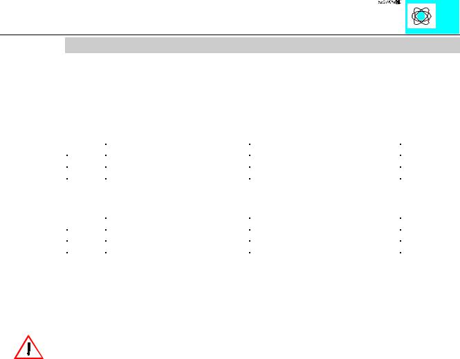
Structure of the inand output data for CAL (from firmware WE)
Mode class 4:
The data is in the 2 Byte objects #BK_AI2W0_XXX, #BK_AI2W1_XXX and #BK_A02W0_XXX. Each module has 2 values.
Input
Mux |
Content |
Description |
|
n |
Input byte0, Input byte1 |
1. and 2. |
Input byte |
n+1 |
Input byte2, Input byte3 |
3. and 4. |
Input byte |
Output |
|
|
|
|
|
|
|
Mux |
Content |
Description |
|
n |
Output byte0, Output byte1 |
1. and 2. |
Output byte |
n+1 |
Output byte2, Output byte3 |
3. and 4. |
Output byte |
Mode class 0:
The description of the data is the same as for class 4 mode. The data is put into objects No.1, No.2 and No.3 (read/write 2 Byte analog).
Attention:
The control byte allows the changing of the registers of the module. It must always be 0 in order to avoid a change in the registers. A wrong mapping can change the function of the module!
Data exchange module 750-654 |
5 |
:$*2Ç, 2Ç6<67(0