Материал: m013209e
Data exchange module
PN 750-654
Technical Description
This technical description is only valid for hardware and software versionx X X X X 2 C 0 0 - - - -. The product series number is printed on the right side of the module.
The operational mode described below is for the factory preset mode.
The following description is preliminary and is applicable to the factory configuration. Many other operational modes are possible (please contact WAGO for the corresponding settings.)
Attention:
Some modules do not provide all power jumper contacts (e.g. 4-channel)! A module which needs all contacts (e.g. 2-channel digital) cannot be connected to the right hand side of modules which do not have 3 power jumper contacts.
The data exchange module is able to run with all :$*2Ç, 2Ç6<67(0 buscouplers (except for the economy type).
Data exchange module 750-654 |
1 |
:$*2Ç, 2Ç6<67(0
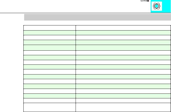
Technical Data
Series 750-
Transmission channel
Transmission rate
Bit transmission
Resistance of cable
Current Consumption (internal)
Transmission length
Input buffer
Output buffer
Voltage supply
Isolation
Bit width internal
Configuration
Operating temperature
Wire connection
Dimensions (mm) W x H x L
Factory preset internal bit width
654
TxD and RxD, full duplex, 2 channel
62500 Baud
via 2 twisted pair with differential signals
120 Ω
65 mA max.
max. 100 m twisted pair
128 Byte
16 Byte
via internal system
500 V System/Supply
1 x 40 bits, 1 x 8 bits control/status
none, parameter configuration with software
0 °C ... + 55 °C
CAGE CLAMP; 0.08 to 2.5 mm²
12 x 64* x 100 (*from upper edge of the carrier rail)
1 x 32 bits in/out, 1 x 8 bits control/status
Data exchange module 750-654 |
2 |
:$*2Ç, 2Ç6<67(0
Description of data exchange module
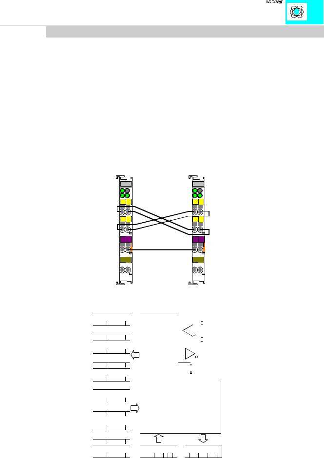
The data exchange module allows the exchange of 4 (5) bytes between different fieldbus systems via multiplexing of a serial connection. The delay which is caused by the multiplexor is < 5ms. The integrated watchdog function switches all outputs to zero if there is no valid information for more than 200 ms via the multiplex connection.
The 128 bytes input buffer provides for high rates of data transmission. When using lower rates of transmission speed you can collect the received data, with less priority, without loosing data.
The 16 byte output buffer provides for faster transmission of larger data strings.
The data exchange module is connected peer-to-peer. For the wiring of the serial multiplex connection the RxD and TxD cables are crossed. The following illustrations show the peer-to-peer connection and the internal structure of the data exchange module.
TxD TxD
+-
RxD RxD
+-
TxD TxD
+-
RxD RxD
+-
M |
M |
S 
 S
S
M |
M |
S  S
S
|
|
|
|
|
|
|
|
|
|
|
|
|
|
|
|
|
|
|
|
|
|
|
|
|
|
|
|
|
|
|
|
|
|
|
|
|
|
|
|
|
|
|
|
:$*2 |
|
|
|
|
|
|
|
|
|
|
|
|
|
|
|
|
:$*2 |
|
|
|
|
|
|
|
|
||||
|
|
|
|
|
|
|
|
|
|
|
|
|
|
|
|
|
|
|
|
|
|
|
|
|
|
|
|
|
|
|
||||||
|
|
|
|
|
|
|
|
|
|
|
|
|
|
|
|
|
|
|
|
|
|
|
|
|
|
|
|
|
|
|
||||||
|
|
|
|
|
|
|
|
|
|
|
|
|
|
|
|
|
|
|
|
|
|
|
|
|
|
|
|
|
|
|
|
|
||||
|
|
|
|
|
|
|
|
|
|
|
|
|
|
|
|
|
|
|
|
|
|
|
|
|
|
|
|
|
|
|
|
|
|
|
|
|
|
|
|
|
|
|
|
|
|
|
|
SHHU WR SHHU FRQQHFWLRQ |
|
|
|
|
|
|
|
|
|||||||||||||||||
|
|
|
|
|
|
|
|
|
|
|
|
|
|
|
|
|
|
|
|
|
|
|
|
|
|
|
|
|
|
|||||||
|
Input byte0 |
|
|
|
|
|
|
Internal |
|
|
|
|
|
|
|
|
|
|
9 |
|
|
|
|
|||||||||||||
|
|
|
|
|
|
|
|
|
|
|
|
|
|
|
|
|
|
|
|
|
|
|
|
|
|
N |
|
|
|
|
||||||
7 |
6 |
5 |
4 |
3 |
2 |
1 |
|
0 |
|
|
|
control system |
|
|
|
|
|
|
|
|
|
|
|
|
|
RxD+ |
||||||||||
|
|
|
|
|
|
|
|
|
|
|
|
|
|
|
|
|
|
|
|
|
|
|
|
|
||||||||||||
|
Input byte1 |
|
|
|
|
|
|
|
|
|
|
|
|
|
|
|
|
|
|
|
|
|
|
|
|
|||||||||||
|
|
|
|
|
|
|
|
|
|
|
|
|
|
|
|
|
|
|
|
|
|
|
|
|
RxD- |
|||||||||||
|
|
|
|
|
|
|
|
|
|
|
|
|
|
|
|
|
|
|
|
|
|
|
|
|
|
|
|
|
|
|
|
|
||||
7 |
6 |
5 |
4 |
3 |
2 |
1 |
|
0 |
|
|
|
|
|
|
|
|
|
|
|
|
|
|
|
|
|
|
|
|
N |
|
|
|
|
|||
|
|
|
|
|
|
|
|
|
|
|
|
|
|
|
|
|
|
|
|
|
|
|
|
|
|
|
|
|
|
|||||||
|
Input byte2 |
|
|
|
|
|
|
|
|
|
|
|
|
|
|
|
|
|
|
|
|
|
|
|
|
TxD+ |
||||||||||
7 |
6 |
5 |
4 |
3 |
2 |
1 |
|
0 |
|
|
|
|
|
|
|
|
|
|
|
|
|
|
|
|
|
|
|
|
|
|
|
|
|
|
|
|
|
|
|
|
|
|
|
|
|
|
|
|
|
|
|
|
|
|
|
|
|
|
|
|
|
|
|
|
|
|
|
|
|
TxD- |
|||
|
Input byte3 |
|
|
|
|
|
|
|
|
|
|
|
|
|
|
|
|
(1 |
|
|
|
|
|
|
||||||||||||
|
|
|
|
|
|
|
|
|
|
|
|
|
|
|
|
|
|
|
|
|
|
|
|
|
|
|
|
|
|
|
M |
|
|
|||
|
|
|
|
|
|
|
|
|
|
|
|
|
|
|
|
|
|
|
|
|
|
|
|
|
|
|
|
|
|
|
|
|
|
|
||
7 |
6 |
5 |
4 |
3 |
2 |
1 |
|
0 |
|
|
|
|
|
|
|
|
|
|
|
|
|
|
|
|
|
|
|
|
|
|
|
|
|
|||
|
|
|
|
|
|
|
|
|
|
|
|
|
|
|
|
|
|
|
|
|
|
|
|
|
|
|||||||||||
|
|
|
|
|
|
|
|
|
|
|
|
|
|
|
|
|
|
|
|
|
|
|
|
|
|
|
|
|
|
|
|
|
S |
|
|
|
|
Input byte4 |
|
|
|
|
|
|
|
|
|
|
|
|
|
|
|
|
|
|
|
|
|
|
|
|
|
|
|||||||||
|
|
|
|
|
|
|
|
|
|
|
|
|
|
|
|
|
|
|
|
|
|
|
|
|
|
|
||||||||||
|
|
|
|
|
|
|
|
|
|
|
|
|
|
|
|
|
|
|
|
|
|
|
|
|
|
|
|
|
||||||||
7 |
6 |
5 |
4 |
3 |
2 |
1 |
|
0 |
|
|
|
|
|
|
|
|
|
|
|
|
|
|
|
|
|
|
|
|
|
|
|
|
|
|
|
|
|
|
|
|
|
|
|
|
|
|
|
|
|
|
|
|
|
|
|
|
|
|
|
|
|
|
|
|
|
|
|
|
|
|
|
|
|
|
Output byte0 |
|
|
|
|
|
|
|
|
|
|
|
|
|
|
|
|
|
|
|
|
|
|
|
|
|
|
|
|
|||||||
7 |
6 |
5 |
4 |
3 |
2 |
1 |
|
0 |
|
|
|
|
|
|
|
|
|
|
|
|
|
|
|
|
|
|
|
|
|
|
|
|
|
|
|
|
|
|
|
|
|
|
|
|
|
|
|
|
|
|
|
|
|
|
|
|
|
|
|
|
|
|
|
|
|
|
|||||||
|
Output byte1 |
|
|
|
|
|
|
|
|
|
|
|
|
|
|
|
|
|
|
|
|
|
|
|
|
|
|
|
|
|||||||
7 |
6 |
5 |
4 |
3 |
2 |
1 |
|
0 |
|
|
|
|
|
|
|
|
|
|
|
|
|
|
|
|
|
|
|
|
|
|
|
|
|
|
|
|
|
|
|
|
|
|
|
|
|
|
|
|
|
|
|
|
|
|
|
|
|
|
|
|
|
|
|
|
|
|
|||||||
|
Output byte2 |
|
|
|
|
|
|
|
|
|
|
|
|
|
|
|
|
|
|
|
|
|
|
|
|
|
|
|
|
|||||||
7 |
6 |
5 |
4 |
3 |
2 |
1 |
|
0 |
|
|
|
|
|
|
|
|
|
|
|
|
|
|
|
|
|
|
|
|
|
|
|
|
|
|
|
|
|
|
|
|
|
|
|
|
|
|
|
|
|
|
|
|
|
|
|
|
|
|
|
|
|
|
|
|
|
|
|||||||
|
Output byte3 |
|
|
|
|
|
|
|
|
|
|
|
|
|
|
|
|
|
|
|
|
|
|
|
|
|
|
|
|
|||||||
7 |
6 |
5 |
4 |
3 |
2 |
1 |
|
0 |
|
|
|
|
|
|
|
|
|
|
|
|
|
|
|
|
|
|
|
|
|
|
|
|
|
|
|
|
|
|
|
|
|
|
|
|
|
|
|
|
|
|
|
|
|
|
|
|
|
|
|
|
|
|
|
||||||||||
|
Output byte4 |
|
|
|
|
|
Control byte |
|
|
|
|
|
|
|
Statusbyte |
|
|
|||||||||||||||||||
7 |
6 |
5 |
4 |
3 |
2 |
1 |
|
0 |
|
|
7 |
|
6 |
5 |
4 |
3 |
2 |
1 |
0 |
|
|
7 |
6 |
|
|
5 |
4 |
|
3 |
2 |
|
1 |
0 |
|||
Data exchange module 750-654 |
3 |
:$*2Ç, 2Ç6<67(0
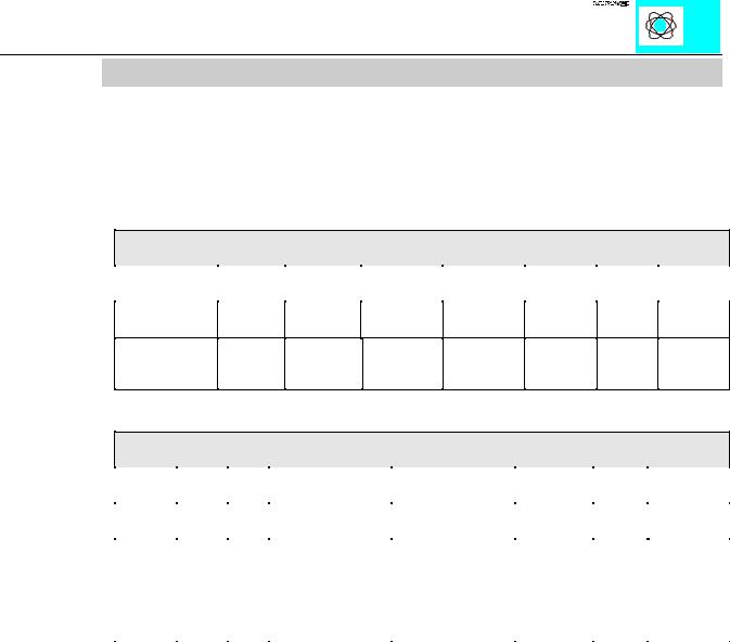
Structure of input and output data:
The module is a combined special function input and output module with 1 x 32 (40) Bit input and output data. The tranfer of the data to be transmitted and the received data is made via up to 5 input and 5 output Bytes. One control byte and one status byte are used to control the floating data.
The control byte consists of the following bits:
Control byte
Bit 7 |
Bit 6 |
Bit 5 |
Bit 4 |
Bit 3 |
Bit 2 |
Bit 1 |
Bit 0 |
|
|
|
|
|
|
|
|
0
Constant value always must be 0
The status byte consists of the following bits:
Status byte
Bit 7 |
Bit 6 |
Bit 5 |
Bit 4 |
Bit 3 |
Bit 2 |
Bit 1 |
Bit 0 |
|
|
|
|
|
|
|
|
0 |
|
|
RCVT1 |
RCVT2 |
CHK |
OVR |
PAR |
|
|
|
|
|
|
|
|
Constant |
|
|
Module is in timeout. |
The receiver is in |
Checksum |
Buffer |
Pariry error or |
value |
|
|
All output bits are set |
timeout. |
error. |
overflow |
wrong data in |
always |
|
|
to 0 (watchdog). |
|
|
|
a frame. |
must be |
|
|
|
|
|
|
|
0. |
|
|
|
|
|
|
|
|
|
|
|
|
|
|
|
The PLC is able to control transmission and reception of data by means of the control byte and the status byte.
Control of the multiplex connection: In the process image of the transmitting buscoupler one Bit is set to „1“ for the whole time. As long as this Bit is „1“ in the receiving coupler, further input Bits can be evaluated. If the Bit is „0“ the multiplex connection has been disrupted. The further Bits are also 0 because of the watchdog.
Control of the multiplex connection with acknowledge: If the transmitting buscoupler gets an acknowledge from the receiving buscoupler, the received bit must be transfered as an output bit to the process image. The transmission is successful as long as the Bit is „1“.
Handshake: If a serial data exchange should be made with the data exchange module, the handshake can be made via „Toggle Bits“. Therefore an input bit and an output bit are reserved. As soon as those bits are different from each other, a request from the opposite module is made. As soon as the request is executed the output bit is toggled.
Data exchange module 750-654 |
4 |
:$*2Ç, 2Ç6<67(0
Structure of the inand output data for Profibus (from firmware WH)
The ID 179 (hex: 0xB3), ( Data consistence over 4 Byte) is used.
Outputs
Byte Description
D0 Output byte0
D1 Output byte1
D2 Output byte2
D3 Output byte3
Inputs
Byte Description
D0 Input byte0
D1 Input byte1
D2 Input byte2
D3 Input byte3
For the ID 188 (hex.: 0xBC), Data consistence over 6 Byte is used, input and output data are now as follows:
Outputs
Byte Description
D0 Control byte
D1 Output byte0
D2 Output byte1
D3 Output byte4
D4 Output byte2
D5 Output byte3
Inputs
Byte Description
D0 Statusbyte
D1 Input byte0
D2 Input byte1
D3 Input byte4
D4 Input byte2
D5 Input byte3
For a S7 PLC the function code SFC14 and SFC15 must be used because the data length is more than 4.
Attention:
The control byte allows the changing of the registers of the module. It must always be 0 in order to avoid a change in the registers. A wrong mapping can change the function of the module!
Data exchange module 750-654 |
5 |
:$*2Ç, 2Ç6<67(0