Материал: 9729

DISCRETE SEMICONDUCTORS
book, halfpage
M3D114
1PS301
High-speed double diode
Product specification |
|
1996 Apr 03 |
|||||
File under Discrete Semiconductors, SC01 |
|
|
|
|
|
|
|
|
|
|
|
|
|
|
|
|
|
|
|
|
|
|
|
|
|
|
|
|
|
|
|

Philips Semiconductors |
Product specification |
|
|
|
|
High-speed double diode |
1PS301 |
|
|
|
|
FEATURES
∙Very small plastic SMD package
∙High switching speed: max. 4 ns
∙Continuous reverse voltage: max. 80 V
∙Repetitive peak reverse voltage: max. 85 V
∙Repetitive peak forward current: max. 500 mA
∙Forward voltage: max. 1.2 V.
APPLICATIONS
∙High-speed switching in e.g. surface mounted circuits.
LIMITING VALUES
DESCRIPTION
The 1PS301 consists of two high-speed switching diodes with common cathodes, fabricated in planar technology, and encapsulated in the very small rectangular plastic SMD SC70 package.
PINNING
PIN |
DESCRIPTION |
|
|
1 |
anode (a1) |
|
|
2 |
anode (a2) |
|
|
3 |
common cathode |
|
|
|
|
2 |
|
1 |
|
|
|
|
|
2 


 1
1
3
3
Top view |
MAM084 |
Marking code: B3.
Fig.1 Simplified outline (SC70) and symbol.
In accordance with the Absolute Maximum Rating System (IEC 134).
SYMBOL |
PARAMETER |
CONDITIONS |
MIN. |
MAX. |
UNIT |
|
|
|
|
|
|
Per diode |
|
|
|
|
|
|
|
|
|
|
|
VRRM |
repetitive peak reverse voltage |
|
− |
85 |
V |
VR |
continuous reverse voltage |
|
− |
80 |
V |
IF |
continuous forward current |
single diode loaded; see Fig.2; |
− |
250 |
mA |
|
|
note 1 |
|
|
|
|
|
|
|
|
|
|
|
double diode loaded; see Fig.2; |
− |
160 |
mA |
|
|
note 1 |
|
|
|
|
|
|
|
|
|
IFRM |
repetitive peak forward current |
|
− |
500 |
mA |
IFSM |
non-repetitive peak forward current |
square wave; Tj = 25 °C prior to |
|
|
|
|
|
surge |
|
|
|
|
|
t = 1 μs |
− |
4 |
A |
|
|
t = 1 s |
− |
0.5 |
A |
|
|
|
|
|
|
Ptot |
total power dissipation |
Tamb = 25 °C; note 1 |
− |
300 |
mW |
Tstg |
storage temperature |
|
−65 |
+150 |
°C |
Tj |
junction temperature |
|
− |
150 |
°C |
Note
1. Device mounted on an FR4 printed-circuit board.
1996 Apr 03 |
2 |

Philips Semiconductors |
|
|
Product specification |
||
|
|
|
|
|
|
High-speed double diode |
|
|
1PS301 |
||
|
|
|
|
|
|
ELECTRICAL CHARACTERISTICS |
|
|
|
|
|
Tj = 25 °C; unless otherwise specified. |
|
|
|
|
|
|
|
|
|
|
|
SYMBOL |
PARAMETER |
CONDITIONS |
TYP. |
MAX. |
UNIT |
|
|
|
|
|
|
Per diode |
|
|
|
|
|
|
|
|
|
|
|
VF |
forward voltage |
see Fig.3 |
|
|
|
|
|
IF = 1 mA |
610 |
− |
mV |
|
|
IF = 10 mA |
740 |
− |
mV |
|
|
IF = 50 mA |
− |
1.0 |
V |
|
|
IF = 100 mA |
− |
1.2 |
V |
IR |
reverse current |
see Fig.4 |
|
|
|
|
|
VR = 25 V |
− |
30 |
nA |
|
|
VR = 80 V |
− |
0.5 |
μA |
|
|
VR = 25 V; Tj = 150 °C |
− |
30 |
μA |
|
|
VR = 80 V; Tj = 150 °C |
− |
100 |
μA |
Cd |
diode capacitance |
f = 1 MHz; VR = 0; see Fig.5 |
− |
1.5 |
pF |
trr |
reverse recovery time |
when switched from IF = 10 mA to |
− |
4 |
ns |
|
|
IR = 10 mA; RL = 100 Ω; |
|
|
|
|
|
measured at IR = 1 mA; see Fig.6 |
|
|
|
Vfr |
forward recovery voltage |
when switched from IF = 10 mA; |
− |
1.75 |
V |
|
|
tr = 20 ns; see Fig.7 |
|
|
|
THERMAL CHARACTERISTICS
SYMBOL |
PARAMETER |
|
CONDITIONS |
VALUE |
UNIT |
|
|
|
|
|
|
Rth j-tp |
thermal resistance from junction to tie-point |
|
|
200 |
K/W |
Rth j-a |
thermal resistance from junction to ambient |
note 1 |
|
415 |
K/W |
Note
1. Device mounted on an FR4 printed-circuit board.
1996 Apr 03 |
3 |
Philips Semiconductors |
Product specification |
|
|
High-speed double diode |
1PS301 |
|
|
GRAPHICAL DATA
MBG444
300 handbook, halfpage
IF
(mA) (1)
200
(2)
100
0
0 |
100 |
Tamb |
o |
C) |
200 |
|
|
( |
|
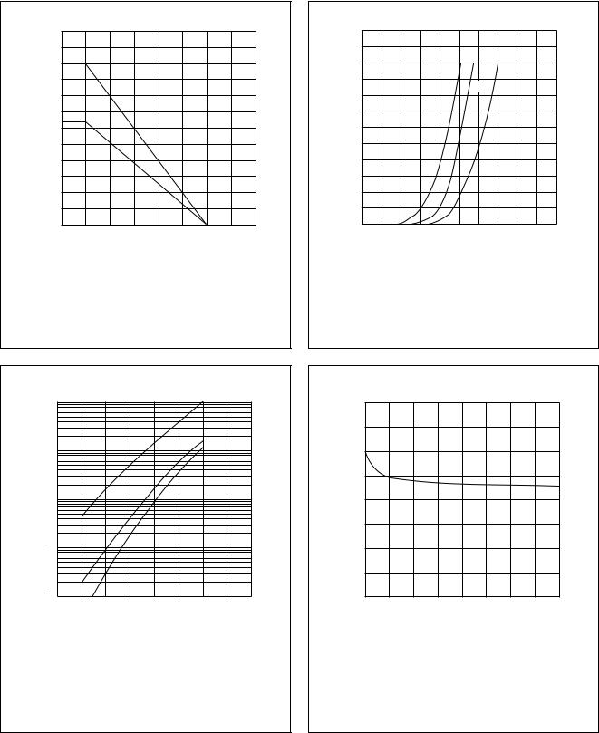
Device mounted on an FR4 printed-circuit board.
(1)Single diode loaded.
(2)Double diode loaded.
Fig.2 Maximum permissible continuous forward current as a function of ambient temperature.
MBG382
300 handbook, halfpage
IF (mA)
(1) |
(2) |
(3) |
200
100
0
0 |
1 |
VF |
(V) |
2 |
|
|
|
(1)Tj = 150 °C; typical values.
(2)Tj = 25 °C; typical values.
(3)Tj = 25 °C; maximum values.
Fig.3 Forward current as a function of forward voltage.
MBG380
102 handbook, halfpage
IR
(μA)
10
(1) |
(2) |
(3) |
1
10 1
10 2
0 |
100 |
Tj |
( |
o |
C) |
200 |
|
|
|
(1)VR = 80 V; maximum values.
(2)VR = 80 V; typical values.
(3)VR = 25 V; typical values.
Fig.4 Reverse current as a function of junction temperature.
MBG446
0.8 handbook, halfpage
Cd (pF)
0.6
0.4
0.2
0
0 |
4 |
8 |
12 VR (V) 16 |
f = 1 MHz; Tj = 25 °C.
Fig.5 Diode capacitance as a function of reverse voltage; typical values.
1996 Apr 03 |
4 |

Philips Semiconductors |
Product specification |
|
|
High-speed double diode |
1PS301 |
|
|
handbook, full pagewidth |
|
t r |
t p |
|
|
|
|
||
|
|
|
t |
|
|
D.U.T. |
10% |
|
|
R = 50 Ω |
IF |
|
I F |
t rr |
S |
|
SAMPLING |
|
t |
|
|
OSCILLOSCOPE |
|
|
|
|
|
|
|
V = VR IF x R S |
|
R i = 50 Ω |
|
|
|
|
|
90% |
(1) |
|
|
VR |
|
|
|
|
|
|
|
|
|
MGA881 |
|
|
input signal |
output signal |
(1) IR = 1 mA.
Fig.6 Reverse recovery voltage test circuit and waveforms.
I |
1 k Ω |
450 Ω |
|
|
I |
90% |
|
V |
|
|
|
|
|
|
RS = 50 Ω |
OSCILLOSCOPE |
|
|
V fr |
|
|
D.U.T. |
Ω |
|
|
|
|
R i = 50 |
|
|
|
|
|
|
10% |
|
|
|
|
MGA882 |
|
|
t |
t |
|
|
t r |
t p |
|
|
|
|
|
input |
|
output |
|
|
|
signal |
|
signal |
Fig.7 Forward recovery voltage test circuit and waveforms.
1996 Apr 03 |
5 |
Смотрите также:
| 05_Холера |
| 10.4. Исследование регистров |
| 1112 |
| 12 |
| 1568 |
| 1673 |
| 17 |
| 1703 |
| 1885 |
| 2. Генераторы постоянного тока |