Материал: sn74hc161
SN54HC161, SN74HC161 4 BIT SYNCHRONOUS BINARY COUNTERS
SCLS297D − JANUARY 1996 − REVISED SEPTEMBER 2003
Clear (L)
Count (H)/
Disable (L)
Load (L)
Count (H)/
Disable (L)
Clock
APPLICATION INFORMATION |
|
|||
|
|
|
LSB |
|
|
CLR |
|
CTR |
|
|
CT=0 |
|
||
|
LOAD |
|
||
|
M1 |
3CT=MAX |
RCO |
|
|
ENT |
|||
|
G3 |
|
||
|
ENP |
|
|
|
|
G4 |
|
|
|
|
CLK |
|
|
|
|
C5/2,3,4+ |
|
||
|
|
|
||
A |
|
1,5D |
[1] |
QA |
B |
|
|
[2] |
QB |
C |
|
|
[3] |
QC |
D |
|
|
[4] |
QD |
|
CLR |
|
CTR |
|
|
CT=0 |
|
||
|
LOAD |
|
||
|
M1 |
3CT=MAX |
RCO |
|
|
ENT |
|||
|
G3 |
|
||
|
ENP |
|
|
|
|
G4 |
|
|
|
|
CLK |
|
|
|
|
C5/2,3,4+ |
|
||
|
|
|
||
A |
|
1,5D |
[1] |
QA |
B |
|
|
[2] |
QB |
C |
|
|
[3] |
QC |
D |
|
|
[4] |
QD |
|
CLR |
|
CTR |
|
|
CT=0 |
|
||
|
LOAD |
|
||
|
M1 |
3CT=MAX |
RCO |
|
|
ENT |
|||
|
G3 |
|
||
|
ENP |
|
|
|
|
G4 |
|
|
|
|
CLK |
|
|
|
|
C5/2,3,4+ |
|
||
|
|
|
||
A |
|
1,5D |
[1] |
QA |
B |
|
|
[2] |
QB |
C |
|
|
[3] |
QC |
D |
|
|
[4] |
QD |
|
CLR |
|
CTR |
|
|
CT=0 |
|
||
|
LOAD |
|
||
|
M1 |
3CT=MAX |
RCO |
|
|
ENT |
|||
|
G3 |
|
||
|
ENP |
|
|
|
|
G4 |
|
|
|
|
CLK |
|
|
|
|
C5/2,3,4+ |
|
||
|
|
|
||
A |
|
1,5D |
[1] |
QA |
B |
|
|
[2] |
QB |
C |
|
|
[3] |
QC |
D |
|
|
[4] |
QD |
To More−Significant Stages
Figure 2
POST OFFICE BOX 655303 • DALLAS, TEXAS 75265 |
11 |
SN54HC161, SN74HC161
4 BIT SYNCHRONOUS BINARY COUNTERS
SCLS297D − JANUARY 1996 − REVISED SEPTEMBER 2003
APPLICATION INFORMATION
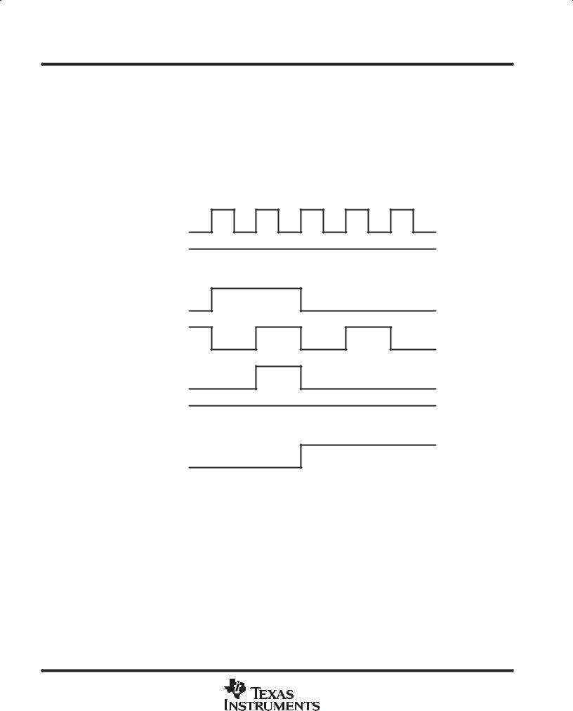
The glitch on RCO is caused because the propagation delay of the rising edge of QA of the second stage is shorter than the propagation delay of the falling edge of ENT. RCO is the product of ENT, QA, QB, QC, and QD (ENT × QA × QB × QC × QD). The resulting glitch is about 7−12 ns in duration. Figure 3 shows the condition in which the glitch occurs. For simplicity, only two stages are being considered, but the results can be applied to other stages. QB, QC, and QD of the first and second stage are at logic one, and QA of both stages are at logic zero (1110 1110) after the first clock pulse. On the rising edge of the second clock pulse, QA and RCO of the first stage go high. On the rising edge of the third clock pulse, QA and RCO of the first stage return to a low level, and QA of the second stage goes to a high level. At this time, the glitch on RCO of the second stage appears because of the race condition inside the chip.
1 |
2 |
3 |
4 |
5 |
CLK
ENT1
QB1, QC1, QD1
QA1
RCO1, ENT2
QB2, QC2, QD2
QA2
RCO2 |
|
|
Glitch (7−12 ns) |
|
|
|
|
Figure 3
The glitch causes a problem in the next stage (stage three) if the glitch is still present when the next rising clock edge appears (clock pulse 4). To ensure that this does not happen, the clock frequency must be less than the inverse of the sum of the clock-to-RCO propagation delay and the glitch duration (tg). In other words,
fmax = 1/(tpd CLK-to-RCO + tg). For example, at 25°C at 4.5-V VCC, the clock-to-RCO propagation delay is 43 ns and the maximum duration of the glitch is 12 ns. Therefore, the maximum clock frequency that the
cascaded counters can use is 18 MHz. The following tables contain the fclock, tw, and fmax specifications for applications that use more than two ’HC161 devices cascaded together.
12 |
POST OFFICE BOX 655303 • DALLAS, TEXAS 75265 |

SN54HC161, SN74HC161 4 BIT SYNCHRONOUS BINARY COUNTERS
SCLS297D − JANUARY 1996 − REVISED SEPTEMBER 2003
APPLICATION INFORMATION
timing requirements over recommended operating free-air temperature range (unless otherwise noted)
|
|
VCC |
TA = 25°C |
SN54HC161 |
SN74HC161 |
UNIT |
|
|
MIN MAX |
MIN MAX |
MIN MAX |
||
|
|
|
|
|||
|
|
|
|
|
|
|
|
|
2 V |
3.6 |
2.5 |
2.9 |
|
|
|
|
|
|
|
|
fclock |
Clock frequency |
4.5 V |
18 |
12 |
14 |
MHz |
|
|
6 V |
21 |
14 |
17 |
|
|
|
|
|
|
|
|
|
|
2 V |
140 |
200 |
170 |
|
tw |
Pulse duration, CLK high or low |
|
|
|
|
ns |
4.5 V |
28 |
40 |
36 |
|||
|
|
6 V |
24 |
36 |
30 |
|
|
|
|
|
|
|
|
switching characteristics over recommended operating free-air temperature range, CL = 50 pF (unless otherwise noted) (see Note 4)
PARAMETER |
FROM |
TO |
VCC |
TA = 25°C |
SN54HC161 |
SN74HC161 |
UNIT |
(INPUT) |
(OUTPUT) |
MIN MAX |
MIN MAX |
MIN MAX |
|||
|
|
|
2 V |
3.6 |
2.5 |
2.9 |
|
fmax |
|
|
|
|
|
|
MHz |
|
|
4.5 V |
18 |
12 |
14 |
||
|
|
|
6 V |
21 |
14 |
17 |
|
|
|
|
|
|
|
|
|
NOTE 4: These limits apply only to applications that use more than two ’HC161 devices cascaded together.
If the ’HC161 devices are used as a single unit, or only two cascaded together, then the maximum clock frequency that the device can use is not limited because of the glitch. In these situations, the device can be operated at the maximum specifications.
A glitch can appear on RCO of a single ’HC161 device, depending on the relationship of ENT to CLK. Any application that uses RCO to drive any input except an ENT of another cascaded ’HC161 device must take this into consideration.
POST OFFICE BOX 655303 • DALLAS, TEXAS 75265 |
13 |
MECHANICAL DATA
|
|
MCFP004A– JANUARY 1995 – REVISED FEBRUARY 2002 |
|
W (R-GDFP-F16) |
|
CERAMIC DUAL FLATPACK |
|
|
0.285 (7,24) |
Base and Seating Plane |
|
0.045 (1,14) |
|
||
0.245 (6,22) |
|
||
0.026 (0,66) |
|
|
|
|
|
0.006 (0,15) |
|
0.080 (2,03) |
|
0.004 (0,10) |
|
0.055 (1,40) |
|
|
|
|
0.305 (7,75) MAX |
|
|
1 |
16 |
0.019 (0,48) |
|
0.015 (0,38) |
|||
|
|
||
|
|
0.050 (1,27) |
|
0.430 (10,92) |
|
|
|
0.370 (9,40) |
|
|
|
|
|
0.005 (0,13) MIN |
|
|
|
4 Places |
|
8 |
9 |
|
|
0.360 (9,14) |
|
0.360 (9,14) |
|
0.250 (6,35) |
|
0.250 (6,35) |
|
|
|
4040180-3/ C 02/02 |
NOTES: A. All linear dimensions are in inches (millimeters).
B.This drawing is subject to change without notice.
C.This package can be hermetically sealed with a ceramic lid using glass frit.
D.Index point is provided on cap for terminal identification only.
E.Falls within MIL STD 1835 GDFP-1F16 and JEDEC MO-092AC
POST OFFICE BOX 655303 • DALLAS, TEXAS 75265 |
1 |