Материал: sn74hc161

SN54HC161, SN74HC161
4 BIT SYNCHRONOUS BINARY COUNTERS
SCLS297D − JANUARY 1996 − REVISED SEPTEMBER 2003
absolute maximum ratings over operating free-air temperature range (unless otherwise noted)†
Supply voltage range, VCC . . . . . . . . . . . . . . . . . . . . . . . . . . . . . . . . . . . . . . . . . . . . . . . . . . . . . . . . . |
. −0.5 V to 7 V |
Input clamp current, IIK (VI < 0 or VI > VCC) (see Note 1) . . . . . . . . . . . . . . . . . . . . . . . . . . . . . . |
. . . . . . ±20 mA |
Output clamp current, IOK (VO < 0 or VO > VCC) (see Note 1) . . . . . . . . . . . . . . . . . . . . . . . . . . |
. . . . . . ±20 mA |
Continuous output current, IO (VO = 0 to VCC) . . . . . . . . . . . . . . . . . . . . . . . . . . . . . . . . . . . . . . . . |
. . . . . . ±25 mA |
Continuous current through VCC or GND . . . . . . . . . . . . . . . . . . . . . . . . . . . . . . . . . . . . . . . . . . . . . |
. . . . . . ±50 mA |
Package thermal impedance, θJA (see Note 2): D package . . . . . . . . . . . . . . . . . . . . . . . . . . . . . |
. . . . . . 73°C/W |
N package . . . . . . . . . . . . . . . . . . . . . . . . . . . . . |
. . . . . . 67°C/W |
NS package . . . . . . . . . . . . . . . . . . . . . . . . . . . |
. . . . . . 64°C/W |
PW package . . . . . . . . . . . . . . . . . . . . . . . . . . . |
. . . . . 108°C/W |
Storage temperature range, Tstg . . . . . . . . . . . . . . . . . . . . . . . . . . . . . . . . . . . . . . . . . . . . . . . . . . . |
−65 °C to 150°C |
†Stresses beyond those listed under “absolute maximum ratings” may cause permanent damage to the device. These are stress ratings only, and functional operation of the device at these or any other conditions beyond those indicated under “recommended operating conditions” is not implied. Exposure to absolute-maximum-rated conditions for extended periods may affect device reliability.
NOTES: 1. The input and output voltage ratings may be exceeded if the input and output current ratings are observed. 2. The package thermal impedance is calculated in accordance with JESD 51-7.
recommended operating conditions (see Note 3)
|
|
|
|
|
|
SN54HC161 |
|
SN74HC161 |
|
UNIT |
||
|
|
|
|
|
|
|
|
|
|
|
|
|
|
|
|
|
|
|
MIN |
NOM |
MAX |
MIN |
NOM |
MAX |
|
|
|
|
|
|
|
|
||||||
|
|
|
|
|
|
|
|
|
|
|
|
|
VCC |
|
Supply voltage |
|
|
|
2 |
5 |
6 |
2 |
5 |
6 |
V |
|
|
|
VCC |
= 2 V |
1.5 |
|
|
1.5 |
|
|
|
|
VIH |
|
High-level input voltage |
VCC |
= 4.5 V |
3.15 |
|
|
3.15 |
|
|
V |
|
|
|
|
VCC |
= 6 V |
4.2 |
|
|
4.2 |
|
|
|
|
|
|
|
VCC |
= 2 V |
|
|
0.5 |
|
|
0.5 |
|
|
VIL |
|
Low-level input voltage |
VCC |
= 4.5 V |
|
|
1.35 |
|
|
1.35 |
V |
|
|
|
|
VCC |
= 6 V |
|
|
1.8 |
|
|
1.8 |
|
|
VI |
|
Input voltage |
|
|
|
0 |
|
VCC |
0 |
|
VCC |
V |
VO |
|
Output voltage |
|
|
|
0 |
|
VCC |
0 |
|
VCC |
V |
|
|
|
VCC |
= 2 V |
|
|
1000 |
|
|
1000 |
|
|
∆ ∆ |
‡ |
Input transition rise/fall time |
V |
CC |
= 4.5 V |
|
|
500 |
|
|
500 |
ns |
t/ v |
|
|
|
|
|
|
|
|
||||
|
|
|
VCC = 6 V |
|
|
400 |
|
|
400 |
|
||
TA |
|
Operating free-air temperature |
|
|
|
−55 |
|
125 |
−40 |
|
85 |
°C |
NOTE 3: All unused inputs of the device must be held at VCC or GND to ensure proper device operation. Refer to the TI application report,
Implications of Slow or Floating CMOS Inputs, literature number SCBA004.
‡If this device is used in the threshold region (from VILmax = 0.5 V to VIHmin = 1.5 V), there is a potential to go into the wrong state from induced grounding, causing double clocking. Operating with the inputs at tt = 1000 ns and VCC = 2 V does not damage the device; however, functionally, the CLK inputs are not ensured while in the shift, count, or toggle operating modes.
6 |
POST OFFICE BOX 655303 • DALLAS, TEXAS 75265 |
SN54HC161, SN74HC161 4 BIT SYNCHRONOUS BINARY COUNTERS
SCLS297D − JANUARY 1996 − REVISED SEPTEMBER 2003
electrical characteristics over recommended operating free-air temperature range (unless otherwise noted)
PARAMETER |
TEST CONDITIONS |
VCC |
|
TA = 25°C |
|
SN54HC161 |
SN74HC161 |
UNIT |
||
MIN |
TYP |
MAX |
MIN MAX |
MIN MAX |
||||||
|
|
|
|
|
||||||
|
|
|
|
|
|
|
|
|
|
|
|
|
|
2 V |
1.9 |
1.998 |
|
1.9 |
1.9 |
|
|
|
|
|
|
|
|
|
|
|
|
|
|
|
IOH = −20 µA |
4.5 V |
4.4 |
4.499 |
|
4.4 |
4.4 |
|
|
VOH |
VI = VIH or VIL |
|
6 V |
5.9 |
5.999 |
|
5.9 |
5.9 |
V |
|
|
|
IOH = −4 mA |
4.5 V |
3.98 |
4.3 |
|
3.7 |
3.84 |
|
|
|
|
IOH = −5.2 mA |
6 V |
5.48 |
5.8 |
|
5.2 |
5.34 |
|
|
|
|
|
2 V |
|
0.002 |
0.1 |
0.1 |
0.1 |
|
|
|
|
|
|
|
|
|
|
|
|
|
|
|
IOL = 20 µA |
4.5 V |
|
0.001 |
0.1 |
0.1 |
0.1 |
|
|
VOL |
VI = VIH or VIL |
|
6 V |
|
0.001 |
0.1 |
0.1 |
0.1 |
V |
|
|
|
IOL = 4 mA |
4.5 V |
|
0.17 |
0.26 |
0.4 |
0.33 |
|
|
|
|
IOL = 5.2 mA |
6 V |
|
0.15 |
0.26 |
0.4 |
0.33 |
|
|
II |
VI = VCC or 0 |
6 V |
|
±0.1 |
±100 |
±1000 |
±1000 |
nA |
||
ICC |
VI = VCC or 0, IO = 0 |
6 V |
|
|
8 |
160 |
80 |
µA |
||
Ci |
|
|
2 V to 6 V |
|
3 |
10 |
10 |
10 |
pF |
|
timing requirements over recommended operating free-air temperature range (unless otherwise noted)
|
|
|
|
|
|
VCC |
TA = 25°C |
SN54HC161 |
SN74HC161 |
UNIT |
|
|
|
|
|
|
|
MIN MAX |
MIN MAX |
MIN MAX |
|
||
|
|
|
|
|
|
|
|
|
|||
|
|
|
|
|
|
|
|
|
|
|
|
|
|
|
|
|
|
2 V |
6 |
4.2 |
5 |
|
|
|
|
|
|
|
|
|
|
|
|
|
|
fclock |
Clock frequency |
4.5 V |
31 |
21 |
25 |
MHz |
|
||||
|
|
|
|
|
|
6 V |
36 |
25 |
29 |
|
|
|
|
|
|
|
|
|
|
|
|
|
|
|
|
|
|
|
|
2 V |
80 |
120 |
100 |
|
|
|
|
|
|
|
|
|
|
|
|
|
|
|
|
CLK high or low |
4.5 V |
16 |
24 |
20 |
|
|
|||
tw |
Pulse duration |
|
|
|
|
6 V |
14 |
20 |
17 |
ns |
|
|
|
|
|
|
|
|
|
|
|||
|
|
|
|
2 V |
80 |
120 |
100 |
|
|||
|
|
|
|
|
|
|
|
||||
|
|
|
|
|
|
|
|
|
|
||
|
|
|
|
low |
4.5 V |
16 |
24 |
20 |
|
|
|
|
|
|
CLR |
|
|
||||||
|
|
|
|
|
|
6 V |
14 |
20 |
17 |
|
|
|
|
|
|
|
|
|
|
|
|
|
|
|
|
|
|
|
|
2 V |
150 |
225 |
190 |
|
|
|
|
|
|
|
|
|
|
|
|
||
|
|
A, B, C, or D |
4.5 V |
30 |
45 |
38 |
|
|
|||
|
|
|
|
|
|
6 V |
26 |
38 |
32 |
|
|
|
|
|
|
|
|
|
|
|
|
|
|
|
|
|
|
|
|
2 V |
135 |
205 |
170 |
|
|
|
|
|
|
|
|
|
|
|
|||
|
|
|
|
|
low |
4.5 V |
27 |
41 |
34 |
|
|
|
|
|
LOAD |
|
|
||||||
tsu |
Setup time before CLK↑ |
|
|
|
|
6 V |
23 |
35 |
29 |
ns |
|
|
|
|
|
|
|
|
|||||
|
|
|
|
2 V |
170 |
255 |
215 |
|
|||
|
|
|
|
|
|
|
|
||||
|
|
|
|
|
|
|
|
|
|||
|
|
ENP, ENT |
4.5 V |
34 |
51 |
43 |
|
|
|||
|
|
|
|
|
|
6 V |
29 |
43 |
37 |
|
|
|
|
|
|
|
|
|
|
|
|
|
|
|
|
|
|
|
|
2 V |
125 |
190 |
155 |
|
|
|
|
|
|
|
|
|
|
|
|||
|
|
|
|
inactive |
4.5 V |
25 |
38 |
31 |
|
|
|
|
|
|
CLR |
|
|
||||||
|
|
|
|
|
|
6 V |
21 |
32 |
26 |
|
|
|
|
|
|
|
|
|
|
|
|
|
|
|
|
|
|
|
|
2 V |
0 |
0 |
0 |
|
|
th |
Hold time, all synchronous inputs after CLK↑ |
|
|
|
|
ns |
|
||||
4.5 V |
0 |
0 |
0 |
|
|||||||
|
|
|
|
|
|
6 V |
0 |
0 |
0 |
|
|
|
|
|
|
|
|
|
|
|
|
|
|
|
|
|
|
|
|
|
|
|
|
|
|
|
|
|
|
|
|
|
|
|
|
|
|
POST OFFICE BOX 655303 • DALLAS, TEXAS 75265 |
7 |

SN54HC161, SN74HC161
4 BIT SYNCHRONOUS BINARY COUNTERS
SCLS297D − JANUARY 1996 − REVISED SEPTEMBER 2003
switching characteristics over recommended operating free-air temperature range, CL = 50 pF (unless otherwise noted) (see Figure 1)
PARAMETER |
FROM |
TO |
VCC |
|
TA = 25°C |
|
SN54HC161 |
SN74HC161 |
UNIT |
||
(INPUT) |
(OUTPUT) |
MIN |
TYP |
MAX |
MIN MAX |
MIN MAX |
|||||
|
|
|
|
|
2 V |
6 |
14 |
|
4.2 |
5 |
|
|
|
|
|
|
|
|
|
|
|
|
|
fmax |
|
|
|
|
4.5 V |
31 |
40 |
|
21 |
25 |
MHz |
|
|
|
|
|
6 V |
36 |
44 |
|
25 |
29 |
|
|
|
|
|
|
|
|
|
|
|
|
|
|
|
|
|
|
2 V |
|
83 |
215 |
325 |
270 |
|
|
|
|
|
|
|
|
|
|
|
|
|
|
|
|
|
RCO |
4.5 V |
|
24 |
43 |
65 |
54 |
|
|
|
CLK |
|
6 V |
|
20 |
37 |
55 |
46 |
|
|
|
|
|
|
|
|
|
|
|
|
||
|
|
2 V |
|
80 |
205 |
310 |
255 |
|
|||
|
|
|
|
|
|
|
|||||
|
|
|
|
|
|
|
|
|
|
|
|
tpd |
|
|
|
Any Q |
4.5 V |
|
25 |
41 |
62 |
51 |
ns |
|
|
|
|
|
6 V |
|
21 |
35 |
53 |
43 |
|
|
|
|
|
|
|
|
|
|
|
|
|
|
|
|
|
|
2 V |
|
62 |
195 |
295 |
245 |
|
|
|
|
|
|
|
|
|
|
|
|
|
|
ENT |
RCO |
4.5 V |
|
17 |
39 |
59 |
49 |
|
||
|
|
|
|
|
6 V |
|
14 |
33 |
50 |
42 |
|
|
|
|
|
|
|
|
|
|
|
|
|
|
|
|
|
|
2 V |
|
105 |
210 |
315 |
265 |
|
|
|
|
|
|
|
|
|
|
|
|
|
|
|
|
|
Any Q |
4.5 V |
|
21 |
42 |
63 |
53 |
|
tPHL |
|
|
|
|
6 V |
|
18 |
36 |
54 |
45 |
ns |
|
CLR |
|
|
|
|
|
|
|
|
||
|
|
|
2 V |
|
110 |
220 |
330 |
275 |
|||
|
|
|
|
|
|
|
|||||
|
|
|
|
|
|
|
|
|
|
|
|
|
|
|
|
RCO |
4.5 V |
|
22 |
44 |
66 |
55 |
|
|
|
|
|
|
6 V |
|
19 |
37 |
56 |
47 |
|
|
|
|
|
|
|
|
|
|
|
|
|
|
|
|
|
|
2 V |
|
38 |
75 |
110 |
95 |
|
tt |
|
|
|
Any |
|
|
|
|
|
|
ns |
|
|
|
4.5 V |
|
8 |
15 |
22 |
19 |
|||
|
|
|
|
|
6 V |
|
6 |
13 |
19 |
16 |
|
|
|
|
|
|
|
|
|
|
|
|
|
operating characteristics, TA = 25°C
|
PARAMETER |
TEST CONDITIONS |
TYP |
UNIT |
|
|
|
|
|
Cpd |
Power dissipation capacitance |
No load |
60 |
pF |
8 |
POST OFFICE BOX 655303 • DALLAS, TEXAS 75265 |
SN54HC161, SN74HC161 4 BIT SYNCHRONOUS BINARY COUNTERS
SCLS297D − JANUARY 1996 − REVISED SEPTEMBER 2003
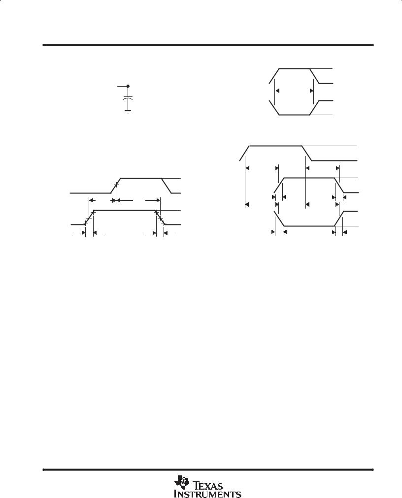
PARAMETER MEASUREMENT INFORMATION
From Output |
Test |
Under Test |
Point |
|
CL = 50 pF |
|
(see Note A) |
LOAD CIRCUIT
Reference |
|
|
50% |
VCC |
|
|
|
|
|||
Input |
|
|
|
||
|
|
|
0 V |
||
|
|
|
|
||
|
|
tsu |
th |
|
|
Data |
|
90% |
90% |
VCC |
|
Input |
50% |
50% |
|||
|
|
||||
|
10% |
|
|
10% 0 V |
|
|
|
tr |
|
tf |
VOLTAGE WAVEFORMS
SETUP AND HOLD AND INPUT RISE AND FALL TIMES
NOTES: A. CL includes probe and test-fixture capacitance.
High-Level |
|
|
|
|
|
|
|
|
50% |
|
|
|
|
|
|
|
|
|
50% |
|
|
|
VCC |
|||||||||||||||||||||||||||
|
|
|
|
|
|
|
|
|
|
|
|
|
|
|
|
|
|
|
|
|
|
|
|
|
|
|
|
|
||||||||||||||||||||||
|
|
|
|
Pulse |
|
|
|
|
|
|
|
|
|
|
|
|
|
|
|
|
|
|
|
|
0 V |
|||||||||||||||||||||||||
|
|
|
|
|
|
|
|
|
|
|
|
|
|
|
|
|
|
|
|
|
|
|
|
|
|
|
|
|
|
|
|
|
|
|||||||||||||||||
|
|
|
|
|
|
|
|
|
|
|
|
|
|
|
|
|
|
|
|
|
|
|
|
|
|
|
|
|
|
|
|
|
|
|
|
|
|
|
|
|
|
|||||||||
|
|
|
|
|
|
|
|
|
|
|
|
|
|
|
|
|
|
|
|
|
|
|
|
|
|
|
|
|
|
|
|
|
|
|
|
|
|
|
|
|
|
|||||||||
|
|
|
|
|
|
|
|
|
|
|
|
|
|
|
|
|
|
|
|
|
|
|
|
|
|
|
|
|
|
|
|
|
|
|
|
|
|
|
|
|
|
|
|
|
|
|
|
|
|
|
Low-Level |
|
|
|
|
|
|
|
|
|
|
|
|
|
|
|
tw |
|
|
|
|
|
|
|
|
|
|
|
|
|
VCC |
||||||||||||||||||||
|
|
|
|
|
|
|
|
|
|
|
|
|
|
|
|
|
|
|
|
|
|
|
|
|
|
|
|
|||||||||||||||||||||||
|
|
|
|
|
|
|
|
50% |
|
|
|
|
|
|
|
|
|
50% |
|
|
|
|||||||||||||||||||||||||||||
|
|
|
|
|
|
|
|
|
|
|
|
|
|
|
|
|
|
|
|
|||||||||||||||||||||||||||||||
|
|
|
|
Pulse |
|
|
|
|
|
|
|
|
|
|
|
|
|
|
|
|
|
|
|
|
0 V |
|||||||||||||||||||||||||
|
|
|
|
|
|
|
|
|
|
|
|
|
|
|
|
|
|
|
|
|
|
|
|
|
|
|
|
|
|
|
|
|
|
|
|
|
|
|
|
|
|
|||||||||
|
|
|
|
|
|
|
|
|
|
|
|
|
|
VOLTAGE WAVEFORMS |
|
|
|
|
|
|
|
|
|
|||||||||||||||||||||||||||
|
|
|
|
|
|
|
|
|
|
|
|
|
|
|
PULSE DURATIONS |
|
|
|
|
|
|
|
|
|
||||||||||||||||||||||||||
Input |
|
|
|
|
50% |
|
|
|
|
|
|
|
|
|
|
|
|
|
|
|
|
|
|
|
50% |
|
|
|
|
|
|
|
|
|
|
|
|
VCC |
||||||||||||
|
|
|
|
|
|
|
|
|
|
|
|
|
|
|
|
|
|
|
|
|
|
|
|
|
|
|
|
|
|
|
|
|
|
|
|
|
|
|
|
|
|
|
|
|
|
|
|
|
|
0 V |
|
|
|
|
|
|
|
|
|
|
|
|
|
|
|
|
|
|
|
|
|
|
|
|
|
|
|
|
|
|
|
|
|
|
|
|
|
|
|
|
|
|
|||||||||
|
|
|
|
|
|
|
|
|
|
|
|
|
|
|
|
|
|
|
|
|
|
|
|
|
|
|
|
|
|
|
|
|
|
|
|
|
|
|
|
|
|
|
|
|
|
|
||||
In-Phase |
|
|
|
|
|
|
|
|
|
tPLH |
|
|
|
|
|
|
|
|
|
|
|
|
|
|
|
|
|
|
|
|
tPHL |
|
|
|
|
|
|
|
|
|
|
VOH |
||||||||
|
|
|
|
|
|
|
|
|
|
|
|
|
|
|
|
|
|
|
|
|
|
|
|
|
|
|
|
|
|
|
|
|
|
|
|
|
|
|||||||||||||
|
|
|
|
|
|
|
|
|
|
|
|
|
|
|
|
|
|
|
|
|
|
|
|
|
|
|
|
|
|
|
|
|
|
|
|
|
|
|
|
|
|
|
|
|
|
|||||
|
|
|
|
|
|
|
|
|
|
|
|
|
|
|
|
|
|
|
|
|
|
|
|
|
|
|
|
|
|
|
|
|
|
|
|
|
|
|
|
|
||||||||||
Output |
|
|
|
|
|
|
|
|
50% |
|
|
|
|
|
90% |
90% |
|
|
|
|
|
50% |
||||||||||||||||||||||||||||
|
|
|
|
|
|
|
|
|
|
|
|
|
|
|
||||||||||||||||||||||||||||||||||||
|
|
|
|
|
|
|
|
|
|
|
|
|
|
|
|
|
|
|
|
|
|
|
|
|
|
|
|
|
|
|
|
|
|
|
||||||||||||||||
|
|
|
|
|
|
|
|
|
|
|
|
10% |
|
|
|
|
|
|
|
|
|
|
|
|
|
|
|
|
|
|
|
|
|
|
|
|
|
|
|
|
|
|
|
|
10% V |
|||||
|
|
|
|
|
|
|
|
|
|
|
|
|
|
|
|
|
|
|
|
|
|
|
|
|
|
|
|
|
|
|
|
|
|
|
|
|
|
|
|
|
|
|
|
|||||||
|
|
|
|
|
|
|
|
|
|
|
|
|
|
|
|
|
|
|
|
|
|
|
|
|
|
|
|
tr |
|
|
|
|
|
|
|
|
|
|
|
|
|
|
|
|
|
|
|
|
|
OL |
|
|
|
|
|
|
|
|
|
|
|
|
|
|
|
|
|
|
|
|
|
|
|
|
|
|
|
|
|
|
|
|
|
|
|
|
|
|
|
|
|
|
|
|
|
|
|
|
|
tf |
|
|
|
|
|
|
|
|
|
|
|
|
|
|
|
|
|
|
|
|
|
|
|
|
|
|
|
|
|
|
|
|
|
|
|
|
|
|
|
|
|
|
|
|
|
|
|
|
|
|||
|
|
|
|
|
|
|
|
|
|
|
|
tPHL |
|
|
|
|
|
|
|
|
|
|
|
|
|
|
|
|
|
|
|
|
|
tPLH |
|
|
|
|
|
|
|
|
|
VOH |
||||||
|
|
|
|
|
|
|
|
|
|
|
|
|
|
|
|
|
|
|
|
|
|
|
|
|
|
|
|
|
|
|
|
|
|
|
|
|
|
|||||||||||||
|
|
|
|
|
|
|
|
|
|
|
|
|
|
|
|
|
|
|
|
|
|
|
|
|
|
|
|
|
|
|
|
|
|
|
|
|
|
|
|
|
|
|
|
|
|
|
|
|
|
|
Out-of-Phase |
|
|
|
|
|
|
|
|
90% |
|
|
|
|
|
|
|
50% |
|
50% |
|
|
|
|
|
90% |
|||||||||||||||||||||||||
|
|
|
|
|
|
|
|
|
|
|
|
|
|
|
|
|
|
|
|
|
|
|
|
|
|
|
|
|
||||||||||||||||||||||
Output |
|
|
|
|
|
|
|
|
|
|
|
|
|
|
|
|
|
|
|
|
10% |
10% |
|
|
|
|
|
|
|
|
|
|
VOL |
|||||||||||||||||
|
|
|
|
|
|
|
|
|
|
|
|
|
|
|
|
|
|
|
|
|
|
|
|
|
|
|
|
|||||||||||||||||||||||
|
|
|
|
|
|
|
|
|
|
|
|
|
|
|
|
|
|
|
|
|
|
|
|
|
|
|
|
|
|
|
|
|||||||||||||||||||
|
|
|
|
|
|
|
|
|
|
|
|
|
|
|
|
|
|
|
|
|
|
|
|
|
|
|
|
|
|
|
|
|
|
|
|
|
|
|
|
|
|
|
|
|
|
|
|
|
|
|
|
|
|
|
|
|
|
|
|
|
|
|
|
|
|
|
|
|
|
|
|
|
|
|
|
|
|
|
tf |
|
|
|
|
|
|
|
|
|
|
|
|
|
|
|
|
|
|
|
|
|
tr |
|
|
|
|
|
|
|
|
|
|
|
|
|
|
|
|
|
|
|
|
|
|
|
|
|
|
|
|
|
|
|
|
|
|
|
|
|
|
|
|
|
|
|
|
|
|
|
|
|
||
VOLTAGE WAVEFORMS
PROPAGATION DELAY AND OUTPUT TRANSITION TIMES
B.Phase relationships between waveforms were chosen arbitrarily. All input pulses are supplied by generators having the following characteristics: PRR ≤ 1 MHz, ZO = 50 Ω, tr = 6 ns, tf = 6 ns.
C.For clock inputs, fmax is measured when the input duty cycle is 50%.
D.The outputs are measured one at a time with one input transition per measurement.
E.tPLH and tPHL are the same as tpd.
Figure 1. Load Circuit and Voltage Waveforms
POST OFFICE BOX 655303 • DALLAS, TEXAS 75265 |
9 |
SN54HC161, SN74HC161
4 BIT SYNCHRONOUS BINARY COUNTERS
SCLS297D − JANUARY 1996 − REVISED SEPTEMBER 2003
APPLICATION INFORMATION
n-bit synchronous counters
This application demonstrates how the look-ahead carry circuit can be used to implement a high-speed n-bit counter. The ’HC161 devices count in binary. Virtually any count mode (modulo-N, N1-to-N2, N1-to-maximum) can be used with this fast look-ahead circuit.
The application circuit shown in Figure 2 is not valid for clock frequencies above 18 MHz (at 25°C and 4.5-V VCC). The reason for this is that there is a glitch that is produced on the second stage’s RCO and every succeeding stage’s RCO. This glitch is common to all HC vendors that Texas Instruments has evaluated, in addition to the bipolar equivalents (LS, ALS, AS).
10 |
POST OFFICE BOX 655303 • DALLAS, TEXAS 75265 |