Материал: mhpm7b8a120arev0
|
|
|
|
|
|
|
Typical Characteristics |
|
||||
(V) |
900 |
TJ = 25°C |
|
|
|
|
|
18 |
|
10000 |
VCE = 600 V |
|
|
|
|
|
|
|
|
|
|
||||
VOLTAGEEMITTER-COLLECTOR |
800 |
I = 8.0 A |
|
|
|
|
|
16 |
V |
ENERGYSWITCHING |
VGE = 15 V |
|
200 |
C |
|
|
|
400 V |
|
4 |
RG = 10 |
Ω |
|||
|
|
|
|
|
|
|
|
|
||||
|
700 |
|
|
|
|
|
14 |
(V) |
(μJ) |
|||
|
600 V |
|
|
|
500 V |
|
|
|
||||
|
|
|
|
|
|
|
|
|
|
|||
|
600 |
|
|
600 V |
|
|
12 |
VOLTAGE |
1000 |
|
TJ =125°C |
|
|
500 V |
|
|
|
|
|
|
|
||||
|
|
|
|
|
|
|
|
|
|
|
||
|
500 |
|
|
|
|
|
10 |
|
|
|
|
|
|
400 V |
|
|
|
|
|
|
|
|
|
||
|
400 |
|
|
|
|
|
8 |
GATE, |
|
|
25°C |
|
|
|
|
|
|
|
|
|
|
||||
|
|
|
|
|
|
|
|
|
|
|
||
|
300 |
|
|
|
|
|
|
6 |
GE |
100 |
|
|
|
|
|
|
|
|
|
|
|
|
|
|
|
, |
|
|
|
|
|
|
|
|
|
|
|
|
CE |
|
|
|
|
|
|
2 |
|
|
|
|
|
V |
100 |
|
|
|
|
|
|
|
|
|
|
|
|
0 |
10 |
20 |
30 |
40 |
50 |
60 |
0 |
|
10 |
|
10 |
|
0 |
70 |
|
1 |
|
|||||||
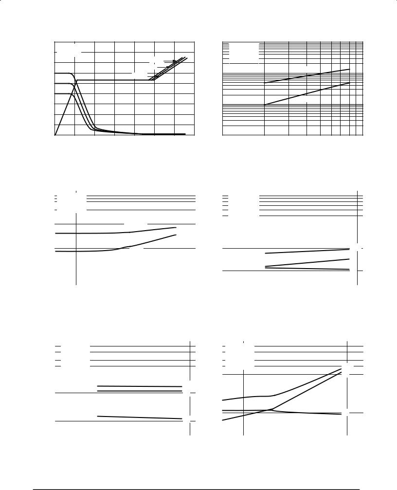
QG, GATE CHARGE (nC)
Figure 8. Gate±to±Emitter Voltage versus
Gate Charge
10000 |
|
|
|
|
|
|
|
|
|
|
|
|
|
|
|
|
|
|
|
|
|
|
|
VCE = 600 V |
|
|
|
|
|
|
|
|
|
|
|
|
|
|
|
|
|
|
|
|
VGE = 15 V |
|
|
|
|
|
|
|
|
|
|
|
|
|
|
|
|
|
(μJ) |
|
|
IC = 8.0 A |
|
|
|
|
|
|
|
|
|
|
|
|
|
|
|
|
|
1000 |
|
|
|
|
|
|
|
|
|
TJ =125°C |
|
|
|
|
|
|
|
|
|
|
ENERGY |
|
|
|
|
|
|
|
|
|
|
|
|
|
|
|
|
|
|
||
SWITCHING |
|
|
|
|
|
|
|
|
|
|
|
|
|
|
|
|
|
|
|
|
|
|
|
|
|
|
|
|
|
|
|
|
|
|
|
|
|
|
|
|
|
100 |
|
|
|
|
|
|
|
|
|
25°C |
|
|
|
|
|
|
|
|
|
|
|
|
|
|
|
|
|
|
|
|
|
|
|
|
|
|
|
|
|
||
|
|
|
|
|
|
|
|
|
|
|
|
|
|
|
|
|
|
|
|
|
|
|
|
|
|
|
|
|
|
|
|
|
|
|
|
|
|
|
|
|
|
|
|
|
|
|
|
|
|
|
|
|
|
|
|
|
|
|
|
|
|
|
|
|
|
|
|
|
|
|
|
|
|
|
|
|
|
|
|
|
|
|
|
|
|
100 |
|
|
|
|
|
|
1000 |
|||||||||||
|
10 |
|
|
|
|
|
|
|||||||||||||
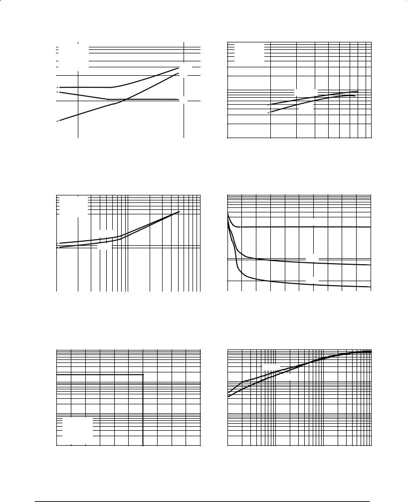
RG, GATE RESISTANCE (Ω)
Figure 10. Inverter Switching Energy E(off) versus Gate Resistance RG
10000 |
|
|
|
|
|
|
|
|
|
|
|
|
|
|
VCE = 600 V |
|
|
|
|
|
|
|
|
|
|
|
VGE = 15 V |
|
|
|
|
|
|
|
|
|
|
|
RG = 10 Ω |
|
|
|
|
|
|
|
|
TIME (ns) |
|
|
TJ = 125°C |
|
|
|
|
|
|
|
|
|
|
|
|
|
|
|
|
|
|
|
|
|
|
|
|
|
|
|
|
|
t(off) |
|
|
SWITCHING |
1000 |
|
|
|
|
|
|
|
|
|
|
|
|
|
|
|
|
|
|
|
|
||
|
|
|
|
|
|
|
|
|
|
tf |
|
|
|
|
|
|
|
|
|
|
|
|
|
|
|
|
|
|
|
|
|
|
|
|
|
|
|
|
|
|
|
|
|
|
|
|
|
|
|
|
|
|
|
|
|
|
|
|
|
|
100 |
|
|
|
|
|
|
|
|
td |
|
|
|
|
|
|
|
|
|
|
|
|
|
|
|
10 |
|||||||||
|
1 |
||||||||||
IC, COLLECTOR CURRENT (A)
Figure 12. Inverter Switching Time tf, td, t(off)
versus Collector Current IC
IC, COLLECTOR CURRENT (A)
Figure 9. Inverter Switching Energy E(off) versus Collector Current IC
|
10000 |
|
|
|
|
|
|
|
|
|
|
|
|
|
|
|
|
|
|
|
|
|
|
|
|
|
|
|
|
VCE = 600 V |
|
|
|
|
|
|
|
|
|
|
|
|
|||||||||
|
|
|
|
VGE = 15 V |
|
|
|
|
|
|
|
|
|
|
|
|
|||||||||
|
|
|
|
RG = 10 Ω |
|
|
|
|
|
|
|
|
|
|
|
|
|||||||||
TIME (ns) |
|
|
TJ = 25°C |
|
|
|
|
|
|
|
|
|
|
|
|
||||||||||
|
|
|
|
|
|
|
|
|
|
|
|
|
|
|
|
|
|
|
|
|
|
|
|
||
SWITCHING |
1000 |
|
|
|
|
|
|
|
|
|
|
|
|
|
|
|
|
|
|
|
|
|
|
|
|
|
|
|
|
|
|
|
|
|
|
|
|
|
|
|
|
|
|
|
|
|
|
|
|
|
|
|
|
|
|
|
|
|
|
|
|
|
|
|
|
|
|
|
|
|
|
|
|
|
|||
|
|
|
|
|
|
|
|
|
|
|
|
|
|
|
|
|
|
|
|
|
|
|
|
||
|
|
|
|
|
|
|
|
|
|
|
|
|
|
|
|
|
|
|
|
t(off) |
|
|
|||
|
|
|
|
|
|
|
|
|
|
|
|
|
|
|
|
|
|
|
|
|
|
|
|
||
|
|
|
|
|
|
|
|
|
|
|
|
|
|
|
|
|
|
|
|
tf |
|||||
|
|
100 |
|
|
|
|
|
|
|
|
|
|
|
|
|
|
|
|
|
td |
|
|
|||
|
|
|
|
|
|
|
|
|
|
|
|
|
|
|
|
|
|
|
|
|
|
|
|
|
|
|
|
|
|
|
|
|
|
|
|
|
|
|
|
|
|
|
|
10 |
|||||||
|
|
1 |
|
|
|
|
|
|
|
|
|
|
|
|
|
|
|
||||||||
|
|
|
|
|
|
IC, COLLECTOR CURRENT (A) |
|
|
|
|
|
|
|
||||||||||||
|
|
|
|
Figure 11. Inverter Switching Time tf, td, t(off) |
|||||||||||||||||||||
|
|
|
|
versus Collector Current IC |
|
|
|
|
|
|
|
||||||||||||||
|
10000 |
|
|
|
|
|
|
|
|
|
|
|
|
|
|
|
|
|
|
|
|
|
|
|
|
|
|
|
|
VCE = 600 V |
|
|
|
|
|
|
|
|
|
|
|
|
|
|
|
|
|
|
|
|
|
|
|
|
|
VGE = 15 V |
|
|
|
|
|
|
|
|
|
|
|
|
|
|
|
|
|
|
|
|
|
|
|
|
|
IC = 8.0 A |
|
|
|
|
|
|
|
|
|
|
|
|
|
|
|
|
|
|
|
|
|
|
|
|
|
TJ = 25°C |
|
|
|
|
|
|
|
|
|
|
|
|
|
|
t |
|
|
|
|
|
|
(ns) |
|
|
|
|
|
|
|
|
|
|
|
|
|
|
|
|
|
|
(off) |
|
|
|
|
|
|
|
|
|
|
|
|
|
|
|
|
|
|
|
|
|
|
|
|
td |
|
|
|
|
|
||
TIME |
|
1000 |
|
|
|
|
|
|
|
|
|
|
|
|
|
|
|
|
|
|
|
|
|
|
|
SWITCHING |
|
|
|
|
|
|
|
|
|
|
|
|
|
|
|
|
|
|
|
|
|
|
|
|
|
|
|
|
|
|
|
|
|
|
|
|
|
|
|
|
|
|
|
|
|
|
|
|
|
|
|
|
|
|
|
|
|
|
|
|
|
|
|
|
|
|
|
|
|
|
|
|
|
|
|
|
|
|
|
|
|
|
|
|
|
|
|
|
|
|
|
|
|
|
|
|
|
|
|
|
|
|
|
|
|
|
|
|
|
|
|
|
|
|
|
|
|
|
|
|
|
|
|
|
|
|
|
|
|
|
|
|
|
|
|
|
|
|
|
|
|
|
|
|
|
|
|
|
|
|
|
|
|
|
|
|
100 |
|
|
|
|
|
|
|
|
|
|
|
|
|
|
|
|
tf |
|
|
|
|
|
||
|
|
|
|
|
|
|
|
|
|
|
|
|
|
|
|
|
|
|
|
|
|
|
|
|
|
|
|
|
100 |
|
|
|
|
|
|
1000 |
|||||||||||||||
|
|
10 |
|
|
|
|
|
|
|||||||||||||||||
RG, GATE RESISTANCE (Ω)
Figure 13. Inverter Switching Time tf,td, t(off)
versus Gate Resistance RG
MHPM7B8A120A |
MOTOROLA |
6 |
|
Typical Characteristics
10000 |
|
|
|
|
|
|
|
|
|
|
|
|
|
|
|
|
|
|
|
|
|
|
|
VCE = 600 V |
|
|
|
|
|
|
|
|
|
|
|
|
|
|
|
|
|
|
|
|
VGE = 15 V |
|
|
|
|
|
|
|
|
|
|
|
|
|
|
|
|
|
|
|
|
IC = 8.0 A |
|
|
|
|
|
|
|
|
|
|
|
t |
|
|
|
|
|
(ns) |
|
|
TJ = 125°C |
|
|
|
|
|
|
|
|
|
|
|
(off) |
|
|
|
|
|
|
|
|
|
|
|
|
|
|
|
|
|
|
|
t |
d |
|
|
|
|
|
TIME |
|
|
|
|
|
|
|
|
|
|
|
|
|
|
|
|
|
|
||
|
|
|
|
|
|
|
|
|
|
|
|
|
|
|
||||||
|
|
|
|
|
|
|
|
|
|
|
|
|
|
|
|
|
|
|
|
|
SWITCHING |
1000 |
|
|
|
|
|
|
|
|
|
|
|
|
|
|
|
|
|
|
|
|
|
|
|
|
|
|
|
|
|
|
|
|
|
|
|
|
|
|
|
|
|
|
|
|
|
|
|
|
|
|
|
|
|
|
|
|
|
|
|
|
|
|
|
|
|
|
|
|
|
|
|
|
|
|
|
|
|
|
|
|
|
|
|
100 |
|
|
|
|
|
|
|
|
|
|
|
|
|
tf |
|
|
|
|
|
|
|
|
|
|
|
|
|
|
|
|
|
|
|
|
|
|
|
|
|
|
|
|
|
|
|
|
|
|
|
|
|
|
|
|
|
|
|
|
|
|
|
|
|
|
|
|
|
|
|
|
|
|
|
|
|
|
|
|
|
|
|
|
|
|
|
|
|
|
|
|
|
|
|
|
|
|
|
|
|
|
|
|
|
|
|
100 |
|
|
|
1000 |
||||||||||||||
|
10 |
|
|
|
||||||||||||||||
RG, GATE RESISTANCE (Ω)
Figure 14. Inverter Switching Time tf, td, t(off)
versus Gate Resistance RG
1000
VCE = 600 V
VGE = 15 V
IC = 8.0 A
TIME (ns) |
|
|
|
|
|
|
|
|
|
|
|
|
|
TJ =125°C |
|
|
|
SWITCHING |
100 |
|
|
|
|
|
|
25°C |
|
|
|
|
10 |
|
|
|
|
|
|
|
|
|
|
|
|
|
|
|
|
|
|
|
|
|
|
|
|
|
|
|
|
|
|
|
|
|
|
|
|
|
|
|
|
|
|
|
|
|
|
|
|
100 |
1000 |
||
|
10 |
||||
RG, GATE RESISTANCE (Ω)
Figure 16. Inverter Switching Time tr
versus Gate Resistance RG
|
1000 |
VCE = 600 V |
|
|
|
|
|
VGE = 15 V |
|
|
RG = 10 Ω |
TIME (ns) |
|
25°C |
SWITCHING |
100 |
|
|
|
TJ =125°C |
|
10 |
10 |
|
1 |
IC, COLLECTOR CURRENT (A)
Figure 15. Inverter Switching Time tr
versus Collector Current IC
10000
(pF) |
1000 |
|
|
|
|
|
Cies |
|
|
|
|
|
|
|
|
|
|
|
|
|
|
|
|
||
|
|
|
|
|
|
|
|
|
|
|
||
CAPACITANCE |
|
|
|
|
|
|
|
|
|
|
|
|
|
|
|
|
|
|
|
|
|
|
|
|
|
|
|
|
|
|
|
|
|
|
|
|
|
|
|
|
|
|
|
|
|
|
|
|
|
|
|
|
|
|
|
|
|
|
|
|
|
|
|
|
|
|
|
|
|
|
|
|
|
|
|
|
|
100 |
|
|
|
|
|
Coes |
|
|
|
|
|
|
|
|
|
|
|
|
|
|
|
|
|
|
|
|
|
|
|
|
|
|
|
|
|
|
|
|
|
|
|
|
|
|
|
|
|
|
|
|
|
|
|
|
|
|
|
|
|
|
|
|
|
|
|
|
|
|
|
|
|
|
|
|
|
|
|
|
10 |
|
|
|
|
|
Cres |
|
|
|
|
|
|
|
|
|
|
|
|
|
|
|
|
|
|
|
20 |
40 |
60 |
80 |
100 |
120 |
140 |
160 |
180 |
200 |
||
|
0 |
|||||||||||
VCE, COLLECTOR±EMITTER VOLTAGE (V)
Figure 17. Output Inverter Capacitance versus Collector Voltage
IC, COLLECTOR CURRENT (A)
100 |
|
|
|
|
|
|
1.0 |
|
|
|
|
|
|
|
|
|
TRANSIENTEFFECTIVETHERMAL |
(NORMALIZED)RESISTANCE |
|
DIODE |
|
|
|
10 |
|
|
|
|
0.1 |
|
IGBT |
|
|||
|
|
|
|
|
|
|
|
||||
|
|
|
|
|
|
|
|
|
|||
1.0 |
+VGE = 15 V |
|
|
|
|
|
0.01 |
|
|
|
|
|
|
|
|
|
|
|
|
|
|
||
|
±VGE = 0 V |
|
|
|
r(t), |
|
|
|
|
|
|
|
RG = 150 Ω |
|
|
|
|
|
|
|
|
||
|
|
|
|
|
|
|
|
|
|
||
0.1 |
TJ = 25°C |
|
|
|
|
0.001 |
|
|
|
||
400 |
800 |
1200 |
1600 |
2000 |
10 |
100 |
1000 |
||||
0 |
|
1 |
|||||||||
|
VCE, COLLECTOR±EMITTER VOLTAGE (V) |
|
|
|
|
t, TIME (ms) |
|
||||
Figure 18. Output Inverter Reversed Biased |
Figure 19. Transient Thermal Resistance |
Safe Operating Area |
|
MOTOROLA |
MHPM7B8A120A |
|
7 |
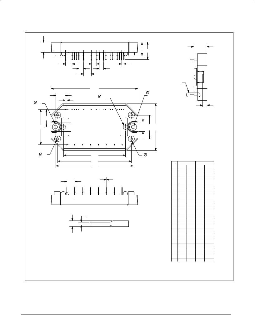
PACKAGE DIMENSIONS
E |
C |
V |
|
K |
|
|
|
|
|
AB |
|
AE |
|
|
|
AA |
|
|
|
|
|
|
|
|
|
|
AC |
|
|
|
AF |
|
9 PL |
|
|
|
|
|
|
|
|
|
|
|
|
|
|
|
|
|
|
|
|
|
|
|
||
|
|
|
|
AD |
|
3 PL |
|
|
|
|
|
|
|
|
|
|
|
|
|
|
|
|
|
|
|
|
|
|
|
|
|
|
|
|
|
|
|
|
|
|
|
|
|
|
DETAIL Z |
|
|
|
||
|
|
|
|
A |
|
|
|
|
|
|
|
|
|
|
|
|
|
|
|
|
|
|
|
|
|
|
Q |
|
|
|
|
|
|
|
N |
G |
|
AH |
|
|
|
|
2 PL |
|
|
|
|
|
||
W |
|
|
2 PL |
|
17 |
|
|
|
|
|
|
|
|
|
||
|
1 |
|
|
|
|
|
|
|
|
|
|
|
|
T |
||
2 PL |
|
|
|
|
|
|
|
|
|
|
|
|
|
|
|
|
L |
|
|
|
|
|
|
|
|
|
|
|
|
|
|
|
|
M |
|
|
|
|
|
|
|
|
S |
R |
B |
|
|
|
|
|
|
|
|
|
|
|
|
|
|
|
|
NOTES: |
|
|
|
|
|
|
|
|
|
|
|
|
|
|
|
|
1. DIMENSIONING AND TOLERANCING PER ANSI |
|||||
|
|
|
|
|
|
|
|
|
|
|
Y14.5M, 1982. |
|
|
|
||
Y |
|
25 |
|
|
|
|
18 |
|
|
X |
2. |
CONTROLLING DIMENSION: MILLIMETER. |
||||
|
|
|
AG |
|
|
|
|
|
3. |
LEAD LOCATION DIMENSIONS (ie: M, B. AA...) |
||||||
4 PL |
|
|
|
|
|
|
|
|
4 PL |
ARE TO THE CENTER OF THE LEAD. |
||||||
|
|
|
P |
|
|
|
|
|
||||||||
|
|
|
|
|
|
|
|
|
|
|
|
MILLIMETERS |
INCHES |
|||
|
|
|
|
U |
|
|
|
|
|
|
|
|
||||
|
|
|
|
|
|
|
|
|
|
|
DIM |
MIN |
MAX |
MIN |
MAX |
|
|
|
|
|
|
|
|
|
|
|
|
|
A |
97.54 |
98.55 |
3.840 |
3.880 |
|
|
|
|
|
|
|
|
|
|
|
|
B |
52.45 |
53.47 |
2.065 |
2.105 |
|
|
|
|
|
|
|
|
|
|
|
|
C |
14.60 |
15.88 |
0.575 |
0.625 |
|
H |
|
|
|
|
J |
|
|
|
|
|
D |
0.43 |
0.84 |
0.017 |
0.033 |
|
|
|
|
|
|
|
|
|
|
E |
10.80 |
12.06 |
0.425 |
0.475 |
||
|
|
|
|
|
25 PL |
|
|
|
|
|
||||||
|
7 PL |
|
|
|
|
|
|
|
|
|
F |
0.94 |
1.35 |
0.037 |
0.053 |
|
|
|
|
|
|
|
|
|
|
|
|
||||||
|
|
|
|
|
|
|
|
|
|
|
|
G |
1.60 |
2.21 |
0.063 |
0.087 |
|
|
|
|
|
|
|
|
|
|
|
|
H |
8.58 |
9.19 |
0.338 |
0.362 |
|
|
|
|
|
|
|
|
|
|
|
|
J |
0.30 |
0.71 |
0.012 |
0.028 |
|
|
|
|
|
|
|
|
|
|
|
|
K |
18.80 |
20.57 |
0.74 |
0.81 |
|
|
|
|
|
|
|
|
|
|
|
|
L |
19.30 |
20.32 |
0.760 |
0.800 |
|
|
|
|
|
|
|
|
|
|
|
|
M |
38.99 |
40.26 |
1.535 |
1.585 |
|
|
|
|
|
|
|
|
|
|
|
|
N |
9.78 |
11.05 |
0.385 |
0.435 |
|
|
|
|
|
|
|
|
|
|
|
|
P |
82.55 |
83.57 |
3.250 |
3.290 |
|
|
|
|
|
|
|
|
|
|
|
|
Q |
4.01 |
4.62 |
0.158 |
0.182 |
|
|
|
|
D |
|
|
|
|
|
|
|
R |
26.42 |
27.43 |
1.040 |
1.080 |
|
|
|
|
|
|
|
|
|
|
|
S |
12.06 |
12.95 |
0.475 |
0.515 |
|
|
|
|
|
|
|
|
|
|
|
|
|
|||||
|
|
F |
|
|
|
|
|
|
|
|
|
T |
4.32 |
5.33 |
0.170 |
0.210 |
|
|
|
|
|
|
|
|
|
|
|
U |
86.36 |
87.38 |
3.400 |
3.440 |
|
|
|
|
|
|
|
|
|
|
|
|
|
V |
14.22 |
15.24 |
0.560 |
0.600 |
|
|
|
|
|
|
|
|
|
|
|
|
W |
7.62 |
8.13 |
0.300 |
0.320 |
|
|
|
|
DETAIL Z |
|
|
|
|
|
|
X |
6.55 |
7.16 |
0.258 |
0.282 |
|
|
|
|
|
|
|
|
|
|
|
Y |
2.49 |
3.10 |
0.098 |
0.122 |
||
|
|
|
|
|
|
|
|
|
|
|
|
AA |
2.24 |
2.84 |
0.088 |
0.112 |
|
|
|
|
|
|
|
|
|
|
|
|
AB |
7.32 |
7.92 |
0.288 |
0.312 |
STYLE 1: |
|
|
|
|
|
|
|
|
|
|
|
AC |
4.78 |
5.38 |
0.188 |
0.212 |
|
|
|
|
|
|
|
|
|
|
|
AD |
8.58 |
9.19 |
0.338 |
0.362 |
|
PIN 1. |
P1 |
PIN 6. |
N2 |
PIN 11. |
G3 |
PIN 16. |
G2 |
PIN 21. |
B |
|
|
|||||
2. |
T± |
7. |
P2 |
12. |
K5 |
17. |
G4 |
22. |
T |
|
|
AE |
6.05 |
6.65 |
0.238 |
0.262 |
3. |
T+ |
8. |
K1 |
13. |
G5 |
18. |
W |
23. |
S |
|
|
AF |
4.78 |
5.38 |
0.188 |
0.212 |
4. |
I+ |
9. |
G1 |
14. |
G6 |
19. |
V |
24. |
R |
|
|
AG |
69.34 |
70.36 |
2.730 |
2.770 |
5. |
I± |
10. |
K3 |
15. |
G7 |
20. |
U |
25. |
N1 |
|
|
AH |
±±± |
5.08 |
±±± |
0.200 |
CASE 440-01
ISSUE O
MHPM7B8A120A |
MOTOROLA |
8 |
|

Motorola reserves the right to make changes without further notice to any products herein. Motorola makes no warranty, representation or guarantee regarding the suitability of its products for any particular purpose, nor does Motorola assume any liability arising out of the application or use of any product or circuit, and specifically disclaims any and all liability, including without limitation consequential or incidental damages. ªTypicalº parameters can and do vary in different applications. All operating parameters, including ªTypicalsº must be validated for each customer application by customer's technical experts. Motorola does not convey any license under its patent rights nor the rights of others. Motorola products are not designed, intended, or authorized for use as components in systems intended for surgical implant into the body, or other applications intended to support or sustain life, or for any other application in which the failure of the Motorola product could create a situation where personal injury or death may occur. Should Buyer purchase or use Motorola products for any such unintended or unauthorized application, Buyer shall indemnify and hold Motorola and its officers, employees, subsidiaries, affiliates, and distributors harmless against all claims, costs, damages, and expenses, and reasonable attorney fees arising out of, directly or indirectly, any claim of personal injury or death associated with such unintended or unauthorized use, even if such claim alleges that Motorola was negligent regarding the design or manufacture of the part. Motorola and  are registered trademarks of Motorola, Inc. Motorola, Inc. is an Equal Opportunity/Affirmative Action Employer.
MOTOROLA |
MHPM7B8A120A |
|
9 |

How to reach us: |
|
|
|
USA/EUROPE: Motorola Literature Distribution; |
JAPAN: Nippon Motorola Ltd.; Tatsumi±SPD±JLDC, Toshikatsu Otsuki, |
||
P.O. Box 20912; Phoenix, Arizona 85036. 1±800±441±2447 |
6F Seibu±Butsuryu±Center, 3±14±2 Tatsumi Koto±Ku, Tokyo 135, Japan. 03±3521±8315 |
||
MFAX: RMFAX0@email.sps.mot.com ±TOUCHTONE (602) 244±6609 |
HONG KONG: Motorola Semiconductors H.K. Ltd.; 8B Tai Ping Industrial Park, |
||
INTERNET: http://Design±NET.com |
51 Ting Kok Road, Tai Po, N.T., Hong Kong. 852±26629298 |
|
|
|
|
||
◊ CODELINE TO BE PLACED HERE |
MHPM7B8A120 /D |
||
|
|
MOTOROLA |
|
10 |
*MHPM7B8A120A/D* |
|