Материал: 9858
DISCRETE SEMICONDUCTORS
k, halfpage
M3D087
PZTM1102
PNP transistor/Schottky-diode module
Product specification |
|
1996 May 09 |
|||||
File under Discrete Semiconductors, SC01 |
|
|
|
|
|
|
|
|
|
|
|
|
|
|
|
|
|
|
|
|
|
|
|
|
|
|
|
|
|
|
|
Philips Semiconductors |
Product specification |
|
|
|
|
PNP transistor/Schottky-diode module |
PZTM1102 |
|
|
|
|
FEATURES
∙Low output capacitance
∙Fast switching time
∙Integrated Schottky protection diode.
APPLICATIONS
∙High-speed switching for industrial applications.
PINNING
PIN |
DESCRIPTION |
|
|
1 |
cathode Schottky |
|
|
2 |
base |
|
|
3 |
emitter |
|
|
4 |
collector, anode Schottky |
|
|
DESCRIPTION
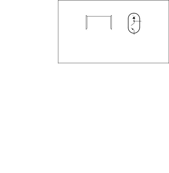
Combination of a PNP transistor and a Schottky barrier diode in a plastic SOT223 package. NPN complement: PZTM1101.
handbook, halfpage |
|
4 |
1 |
|
||||
|
|
|
|
|
|
|
|
|
4
|
|
|
|
|
|
|
|
|
|
2 |
|
|
|
|
|
|
|
|
|
|
|
|
|
|
|
|
|
1 |
|
2 |
|
3 |
3 |
|||||
Top view |
|
|
|
|
||||||||
|
|
|
|
MAM237 |
||||||||
Marking code: TM1102.
Fig.1 Simplified outline (SOT223) and symbol.
LIMITING VALUES
In accordance with the Absolute Maximum Rating System (IEC 134).
SYMBOL |
PARAMETER |
CONDITIONS |
MIN. |
MAX. |
UNIT |
|
|
|
|
|
|
|
|
PNP transistor |
|
|
|
|
||
|
|
|
|
|
|
|
VCBO |
collector-base voltage |
open emitter |
− |
−40 |
V |
|
VCES |
collector-emitter voltage |
VBE = 0 |
− |
−40 |
V |
|
VEBO |
emitter-base voltage |
open collector |
− |
−6 |
V |
|
IC |
collector current (DC) |
|
− |
−200 |
mA |
|
Schottky barrier diode |
|
|
|
|
||
|
|
|
|
|
|
|
VR |
continuous reverse voltage |
|
− |
40 |
V |
|
IF |
forward current (DC) |
|
− |
1 |
A |
|
IF(AV) |
average forward current |
|
− |
1 |
A |
|
P |
power dissipation |
up to Tamb = 25 °C; note 1 |
− |
0.5 |
W |
|
Tj |
junction temperature |
reverse current applied |
− |
125 |
°C |
|
|
|
|
forward current applied |
− |
150 |
°C |
|
|
|
|
|
|
|
Combined device |
|
|
|
|
||
|
|
|
|
|
|
|
Ptot |
total power dissipation |
up to Tamb = 25 °C; note 2 |
− |
1.2 |
W |
|
Tamb |
operating ambient temperature |
|
−55 |
+150 |
°C |
|
Tstg |
storage temperature |
|
−55 |
+150 |
°C |
|
Tj |
junction temperature |
|
− |
150 |
°C |
|
Notes
1.An additional copper area of >20 mm2 is required for pin 1, if power dissipation in the Schottky die is >0.5 W.
2.It is not allowed to dissipate the total power of 1.2 W in the Schottky die only.
1996 May 09 |
2 |

Philips Semiconductors |
|
|
Product specification |
|||
|
|
|
|
|
|
|
PNP transistor/Schottky-diode module |
|
PZTM1102 |
||||
|
|
|
|
|
|
|
ELECTRICAL CHARACTERISTICS |
|
|
|
|
||
Tamb = 25 °C unless otherwise specified. |
|
|
|
|
||
|
|
|
|
|
|
|
SYMBOL |
PARAMETER |
CONDITIONS |
MIN. |
MAX. |
UNIT |
|
|
|
|
|
|
|
|
NPN transistor |
|
|
|
|
||
|
|
|
|
|
|
|
V(BR)CBO |
collector-base breakdown |
open emitter; IC = −10 μA; IE = 0; |
−40 |
− |
V |
|
|
voltage |
Tamb = −55 to +150 °C; note 1 |
|
|
|
|
V(BR)CES |
collector-emitter |
open base; IC = −1 mA; VBE = 0; |
−40 |
− |
V |
|
|
breakdown voltage |
Tamb = −55 to +150 °C; note 1 |
|
|
|
|
V(BR)EBO |
emitter-base breakdown |
open collector; IE = −10 μA; IC = 0; |
−6 |
− |
V |
|
|
voltage |
Tamb = −55 to +150 °C; note 1 |
|
|
|
|
ICES |
collector-emitter cut-off |
VCE = −20 V; VBE = 0 |
− |
100 |
nA |
|
|
current |
|
VCE = −20 V; VBE = 0; Tamb = −55 to +150 °C |
− |
50 |
μA |
IEBO |
emitter-base cut-off current |
VEB = −6 V; IC = 0 |
− |
50 |
nA |
|
|
|
|
VEB = −6 V; IC = 0; Tamb = −55 to +150 °C |
− |
10 |
μA |
VCEsat |
collector-emitter saturation |
note 1 |
|
|
|
|
|
voltage |
IC = −10 mA; IB = −1 mA |
− |
−200 |
mV |
|
|
|
|
IC = −50 mA; IB = −3.2 mA |
− |
−300 |
mV |
VCEsat |
collector-emitter saturation |
Tamb = −55 to +150 °C; note 1 |
|
|
|
|
|
voltage |
IC = −10 mA; IB = −1 mA |
− |
−250 |
mV |
|
|
|
|
IC = −50 mA; IB = −3.2 mA |
− |
−350 |
mV |
VBEsat |
base-emitter saturation |
note 1 |
|
|
|
|
|
voltage |
IC = −10 mA; IB = −1 mA |
− |
−850 |
mV |
|
|
|
|
IC = −50 mA; IB = −5 mA |
− |
−950 |
mV |
VBEsat |
base-emitter saturation |
Tamb = −55 to +150 °C; note 1 |
|
|
|
|
|
voltage |
IC = −10 mA; IB = −1 mA |
− |
−1.0 |
V |
|
|
|
|
IC = −50 mA; IB = −5 mA |
− |
−1.1 |
V |
Cob |
output capacitance |
IE = ie = 0; VCB = −5 V; f = 1 MHz |
− |
4.5 |
pF |
|
Cib |
input capacitance |
IC = ic = 0; VEB = −0.5 V; f = 1 MHz |
− |
10 |
pF |
|
fT |
transition frequency |
IC = −10 mA; VCE = −20 V; f = 100 MHz |
250 |
− |
MHz |
|
hFE |
DC current gain |
VCE = −1 V; note 1 |
|
|
|
|
|
|
|
IC = −0.1 mA |
40 |
− |
|
|
|
|
IC = −1 mA |
70 |
− |
|
|
|
|
IC = −10 mA |
100 |
300 |
|
|
|
|
IC = −100 mA |
30 |
− |
|
hFE |
DC current gain |
VCE = −1 V; Tamb = −55 to +150 °C; note 1 |
|
|
|
|
|
|
|
IC = −10 mA |
60 |
500 |
|
|
|
|
IC = −100 mA |
15 |
− |
|
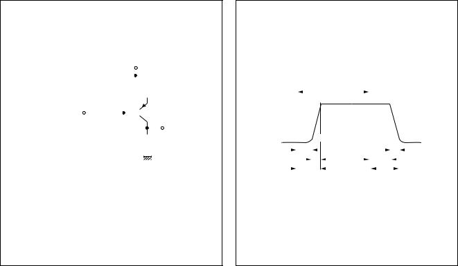
SWITCHING TIMES (see Figs 2 and 3) |
|
|
|
|
||
|
|
|
|
|
|
|
td |
delay time |
VCC = 5 V |
3 |
7 |
ns |
|
tr |
rise time |
IC = 50 mA |
13 |
23 |
ns |
|
ts |
storage time |
Vi = 0 to 5 V |
200 |
380 |
ns |
|
tf |
fall time |
|
50 |
80 |
ns |
|
1996 May 09 |
3 |

Philips Semiconductors |
|
|
Product specification |
|||
|
|
|
|
|
|
|
PNP transistor/Schottky-diode module |
|
PZTM1102 |
||||
|
|
|
|
|
|
|
|
|
|
|
|
|
|
SYMBOL |
PARAMETER |
CONDITIONS |
MIN. |
MAX. |
UNIT |
|
|
|
|
|
|
|
|
Schottky barrier diode |
|
|
|
|
||
|
|
|
|
|
|
|
VF |
forward voltage |
IF = 100 mA; note 1 |
− |
330 |
mV |
|
|
|
|
IF = 100 mA; Tamb = −55 to +150 °C; note 1 |
− |
400 |
mV |
|
|
|
IF = 1 A; note 1 |
− |
500 |
mV |
|
|
|
IF = 1 A; Tamb = −55 to +150 °C; note 1 |
− |
560 |
mV |
IR |
reverse current |
VR = 40 V; note 1 |
− |
300 |
μA |
|
|
|
|
VR = 40 V; Tj = 125 °C; |
− |
35(2) |
mA |
|
|
|
Tamb = −55 to +150 °C; note 1 |
|
|
|
IR |
reverse current |
VR = 10 V; note 1 |
− |
40 |
μA |
|
|
|
|
VR = 10 V; Tj = 125 °C; |
− |
15(2) |
mA |
|
|
|
Tamb = −55 to +150 °C; note 1 |
|
|
|
Cj |
junction capacitance |
VR = 0 V; f = 1 MHz |
− |
250 |
pF |
|
Notes
1.Measured under pulsed conditions: tp ≤ 300 μs; δ ≤ 0.01.
2.Limiting value for Tj = 125 °C; Tj = 150 °C with reverse current applied is not allowed as this may cause thermal runaway leading to thermal destruction of the diode. A peak junction temperature of Tj = 150 °C is only allowed with forward voltage applied.
THERMAL CHARACTERISTICS
SYMBOL |
PARAMETER |
CONDITIONS |
VALUE |
UNIT |
|
|
|
|
|
Rth j-a |
thermal resistance from junction to ambient (for the transistor) |
note 1 |
100 |
K/W |
Rth j-a |
thermal resistance from junction to ambient (for the Schottky diode) |
note 1 |
250 |
K/W |
Note
1. Refer to SOT223 standard mounting conditions.
1996 May 09 |
4 |
Philips Semiconductors |
Product specification |
|
|
PNP transistor/Schottky-diode module |
PZTM1102 |
|
|
GRAPHICAL DATA |
|
|
|
|
|
|
|
|
|
|
|
|
|
|
|
|
|
|
|
|
|
|
|
|
|
handbook, halfpage |
|
|
|
|
|
|
|
|
|
|
|
|
|
|
|
|
|
|
|
|
|
|
|
|
|
|
|
|
|
|
|
|
|
|
|
5 V |
|
|
|
|
|
|
|
|
|
|
|
|
|
|
|
|
|
|
|
|
|
|
|
|
|
|
|
|
|
|
|
|
|
|
|
|
|
|
|
|
|
|
|
|
|
|
|
|
|
|
|
|
|
|
|
|
|
|
|
|
|||
|
|
|
|
|
|
|
|
|
|
|
|
|
|
|
|
|
|
|
|
|
|
|
|
|
|
|
|
|
|
|
|
|
|
|
|
|
|
|
|
|
|
|
|
|
|
|
|
|
|
|
|
|
|
|
|
|
|||||
handbook, halfpage |
|
|
|
|
|
|
|
|
|
|
VCC = 5 V DC |
INPUT |
|
|
|
|
|
|
|
|
|
|
|
|
|
|
|
|
|
|
|
|
|
|
|
|
|
|
|
|
|
|
|
|
|
|
|
||||||||||||||
|
|
|
|
|
|
|
|
|
|
|
|
|
|
|
|
|
|
|
|
|
|
|
|
Vi |
|
|
|
|
|
|
|
|
|
|
|
|
|
|
|
|
|
|
|
|
|
|
|
|
|
|
|
|
|
|
|
|
|
|
0 V |
||
|
|
|
|
|
|
|
|
|
7.5 kΩ |
|
|
|
|
|
|
|
|
|
5.23 Ω |
|
|
|
|
|
|
|
|
|
|
|
|
|
|
|
|
|
|
|
|
|
|
|
|
|
|
|
|
|
|
|
|
|
|
||||||||
|
|
|
|
|
|
|
|
|
|
|
|
|
|
|
|
|
|
|
|
|
|
|
|
|
|
|
|
|
tp |
|
|
|
|
|
|
|
|
|
|
|
|
|
|
|
|
|
|
|
|
|
|
||||||||||
|
|
|
|
|
|
|
|
|
|
|
|
|
|
|
|
|
|
|
|
|
|
|
|
|
|
|
|
|
|
|
|
|
|
|
|
|
|
|
|
|
|
|
|
|
|
|
|
|
|
||||||||||||
5 V |
|
|
|
|
|
|
|
|
|
(5%) |
|
|
|
|
|
|
|
|
(1%) |
Vo |
|
|
|
|
|
|
|
|
|
|
|
|
|
|
|
|
|
|
|
|
|
|
|
10% |
|
|
|
||||||||||||||
|
|
|
|
|
|
|
|
|
|
|
|
|
|
|
|
|
|
|
|
|
|
|
|
|
|
|
|
|
|
|
|
|
|
|
|
|
|
|
|
|
|
|
|
|
|||||||||||||||||
|
|
|
|
|
Vi |
|
|
|
|
|
|
|
|
|
|
|
|
|
|
DUT |
|
|
|
|
|
|
90% |
|
|
|
|
|
|
|
|
|
|
|
|
|
|
|
|
||||||||||||||||||
|
|
|
|
|
|
|
|
|
|
|
|
|
|
|
|
|
|
|
|
|
|
|
|
|
|
|
|
|
|
|
|
|
|
|
|
|
|
|
|
|
|||||||||||||||||||||
0 V |
|
|
|
825 |
Ω |
|
|
|
|
|
|
Vo (pin 4) |
OUTPUT |
|
|
|
|
|
|
|
|
|
|
|
|
|
|
|
|
|
|
|
|
|
|
|
|
|
|
|
|
|
|
|
|
|
|
|
|||||||||||||
|
|
(1%) |
|
|
|
|
|
|
|
|
|
|
|
|
|
|
|
|
|
|
|
|
|
|
|
|
|
|
|
|
|
|
|
|
|
|
|
|
|
|
|
|
|
|
|
|
|
|
|
||||||||||||
|
|
|
|
|
|
|
|
|
|
|
|
|
|
|
|
|
|
|
|
|
|
|
|
|
|
|
|
|
|
|
|
|
|
|
|
|
|
|
|
|
|
|
|
|
|
|
|
|
|
|
|
||||||||||
|
|
|
|
|
|
|
|
|
|
|
|
|
|
|
|
|
|
|
|
|
|
90 Ω |
|
|
|
|
|
|
|
|
10% |
|
|
|
|
|
|
|
|
|
|
|
|
|
|
|
|
|
90% |
|
|
||||||||||
|
|
|
|
|
|
|
|
|
|
|
|
|
|
|
|
|
|
|
|
|
|
|
|
|
|
|
|
|
|
|
|
|
|
|
|
|
|
|
|
|
|
|
|
|
|
|
|||||||||||||||
|
|
|
|
|
|
|
|
|
|
|
|
|
|
|
|
|
|
|
|
|
(1%) |
td |
|
|
|
|
|
|
|
|
|
|
|
|
|
|
|
|
|
|
|
|
|
|
|
|
|
|
|
|
|
|
|
|
tf |
||||||
|
|
|
|
|
|
|
|
|
|
|
|
|
|
|
|
|
|
|
|
|
|
|
MBH222 |
|
|
|
|
|
|
|
|
|
|
|
tr |
|
|
|
ts |
|
|
|
|
|
|
|
|
||||||||||||||
|
|
|
|
|
|
|
|
|
|
|
|
|
|
|
|
|
|
|
|
|
|
|
|
|
|
|
|
|
|
|
|
|
|
|
|
|
|
|
|
|
|
|
|
|
|
|
|
|
|
|
|
|
|
|
|
|
|
|
|
|
|
|
|
|
|
|
|
|
|
|
|
|
|
|
|
|
|
|
|
|
|
|
|
|
|
|
|
|
|
|
|
|
ton |
|
|
|
|
|
|
|
|
|
|
|
toff |
|
|
|
|
|
|
|
|
|
|
MBH223 |
|||||||
|
|
|
|
|
|
|
|
|
|
|
|
|
|
|
|
|
|
|
|
|
|
|
|
|
|
|
|
|
|
|
|
|
|
|
|
|
|
|
|
|
|
|
|
|
|
|
|
|
|
|
|
||||||||||
tr < 5 ns (10% to 90%); tp = 1 μs; δ = 0.02; Zi = 50 Ω. ton = td + tr; toff = ts + tf.
Fig.2 Switching times test circuit. |
Fig.3 Input and output waveforms. |
1996 May 09 |
5 |